PI3B16213V Ver la hoja de datos (PDF) - Pericom Semiconductor
Número de pieza
componentes Descripción
Lista de partido
PI3B16213V Datasheet PDF : 4 Pages
| |||
PI3B16213 111222333444555666777888999000111222333444555666777888999000111222333444555666777888999000111222111222333444555666777888999000111222333444555666777888999000111222333444555666777888999000111222111222333444555666777888999000111222333444555666777888999000111222333444555666777888999000111222111222333444555666777888999000111222333444555666777888999000111222333444555666777888999000111222111222333444555666777888999000111222
3.3V, 24-Bit Bus-Exchange Switch
Product Features
Near-zero propagation delay
5-ohm switches connect inputs to outputs
Direct bus connection when switches are ON
Fast Switching Speed: 5.5ns max.
Operating VCC Range: 3.0V to 3.6V
Industrial operating temperature: 40°C to +85°C
Packages available:
56-pin 240-mil wide thin plastic TSSOP (A)
56-pin 300-mil wide plastic SSOP (V)
Product Description
Pericom Semiconductors PI3B series of logic circuits are produced
using the Companys advanced submicron CMOS technology.
The PI3B16213 is a 3.3 volt, 24-bit bus-exchange switch designed
with a low ON resistance allowing connections to be made with
minimal propagation delay. This device operates either as a 24-bit
or as a 12-bit bus switch, providing data exchange between the four
signal ports via the data-select (S0-S2) terminals.
Logic Block Diagram
Product Pin Configuration
1 of 12 Channels
XA1
XB1
XA2
XB2
FLOW CONTROL
S0
S1
S2
Truth Table
Function
S2 S1
Disconnect
LL
A1 to B1
LL
A1 to B2
LH
A2 to B1
LH
A2 to B2
HL
A1 to A2 and B2
HL
A1 to B1, A2 to B2 H H
A1 to B2, A2 to B1 H H
Note:
1. H = High Voltage Level
L = Low Voltage Level
Z = High Impedance
S0 A1
A2
L
Z
Z
H
B1
Z
L
B2
Z
H
Z
B1
L
Z
B2
H A2/B2 A1/B2
L
B1
B2
H
B2
B1
S0
1A1
1A2
2A1
2A2
3A1
3A2
GND
4A1
4A2
5A1
5A2
6A1
6A2
7A1
7A2
VCC
8A1
GND
8A2
9A1
9A2
10A1
10A2
11A1
11A2
12A1
12A2
1
56
2
55
3
54
4
53
5
52
6
51
7
50
8
49
9
48
10
47
11 56-Pin 46
12 A, V 45
13
44
14
43
15
42
16
41
17
40
18
39
19
38
20
37
21
36
22
35
23
34
24
33
25
32
26
31
27
30
28
29
S1
S2
1B1
1B2
2B1
2B2
3B1
GND
3B2
4B1
4B2
5B1
5B2
6B1
6B2
7B1
7B2
8B1
GND
8B2
9B1
9B2
10B1
10B2
11B1
11B2
12B1
12B2
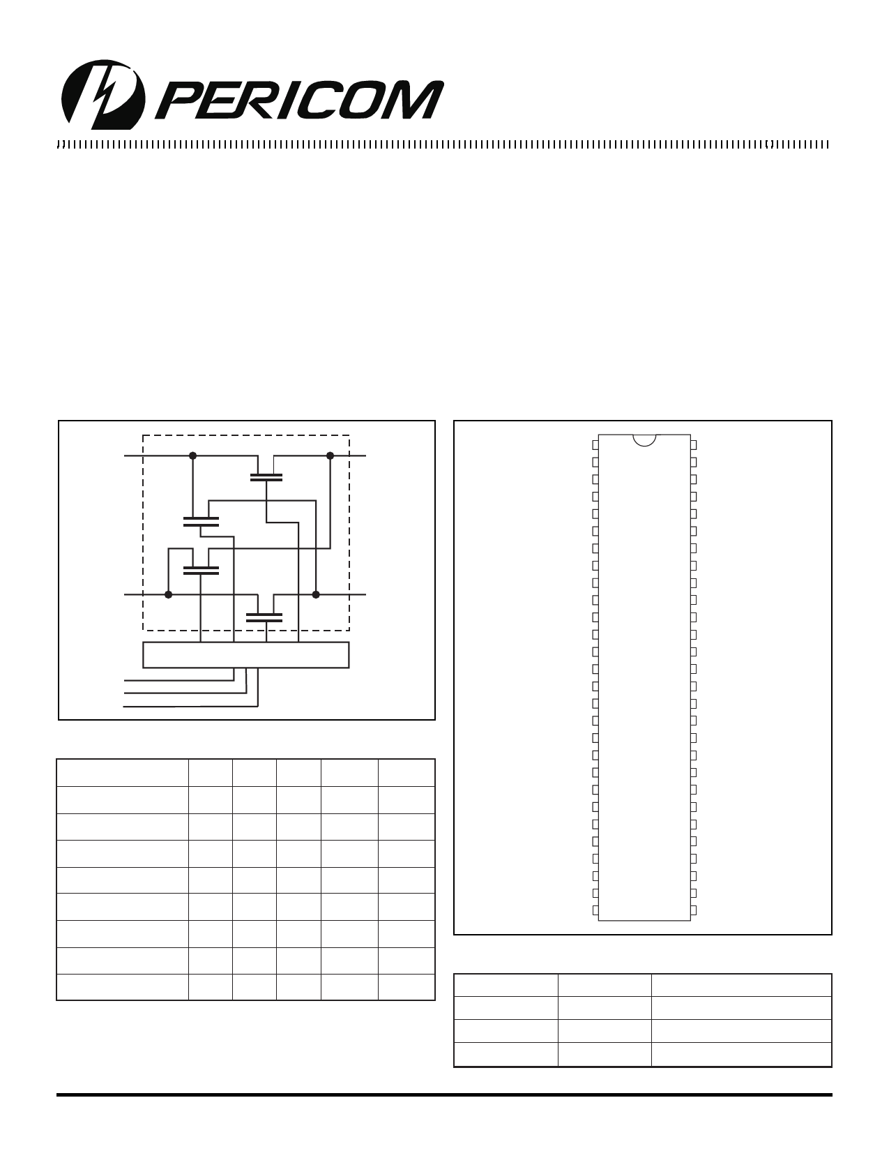
Product Pin Description
Pin Name
I/O
S0-S2
I
xAx
I/O
xBx
I/O
Description
Select Inputs
Bus A
Bus B
1
PS8169A 08/21/01
Share Link: 