CDB4396 Ver la hoja de datos (PDF) - Cirrus Logic
Número de pieza
componentes Descripción
Lista de partido
CDB4396 Datasheet PDF : 28 Pages
| |||
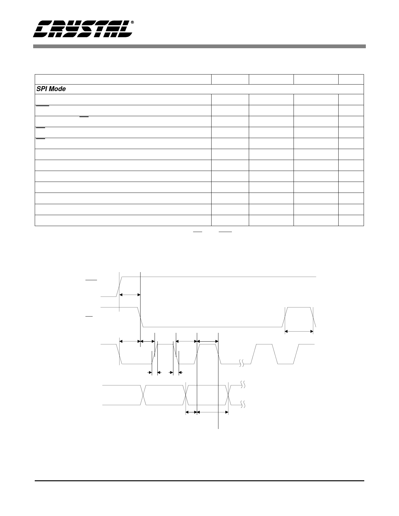
CS4396
SWITCHING CHARACTERISTICS - CONTROL PORT
(TA = 25 °C; VD = 5.25 V to 3.0 Volts; Inputs: logic 0 = AGND, logic 1 = VD, CL = 30 pF)
Parameter
Symbol
Min
Max
SPI Mode
CCLK Clock Frequency
fsclk
-
6
RST Rising Edge to CS Falling
tsrs
500
-
CCLK Edge to CS Falling
(Note 9)
tspi
500
-
CS High Time Between Transmissions
tcsh
1.0
-
CS Falling to CCLK Edge
tcss
20
-
CCLK Low Time
tscl
66
-
CCLK High Time
tsch
66
-
CDIN to CCLK Rising Setup Time
tdsu
40
-
CCLK Rising to DATA Hold Time
(Note 10)
tdh
15
-
Rise Time of CCLK and CDIN
(Note 11)
tr2
-
100
Fall Time of CCLK and CDIN
(Note 11)
tf2
-
100
CCLK Falling to CDOUT valid
tov
45
Unit
MHz
ns
ns
µs
ns
ns
ns
ns
ns
ns
ns
ns
Notes: 9. tspi only needed before first falling edge of CS after RST rising edge. tspi = 0 at all other times.
10. Data must be held for sufficient time to bridge the transition time of CCLK.
11. For FSCK < 1 MHz
RST
t srs
CS
CCLK
CDIN
t spi t css
t scl t sch
t r2
t f2
t dsu t dh
Figure 3. SPI Control Port Timing
t csh
10
DS288PP1
Share Link: 