CS5334 Ver la hoja de datos (PDF) - Cirrus Logic
Número de pieza
componentes Descripción
Lista de partido
CS5334 Datasheet PDF : 20 Pages
| |||
CS5334 CS5335
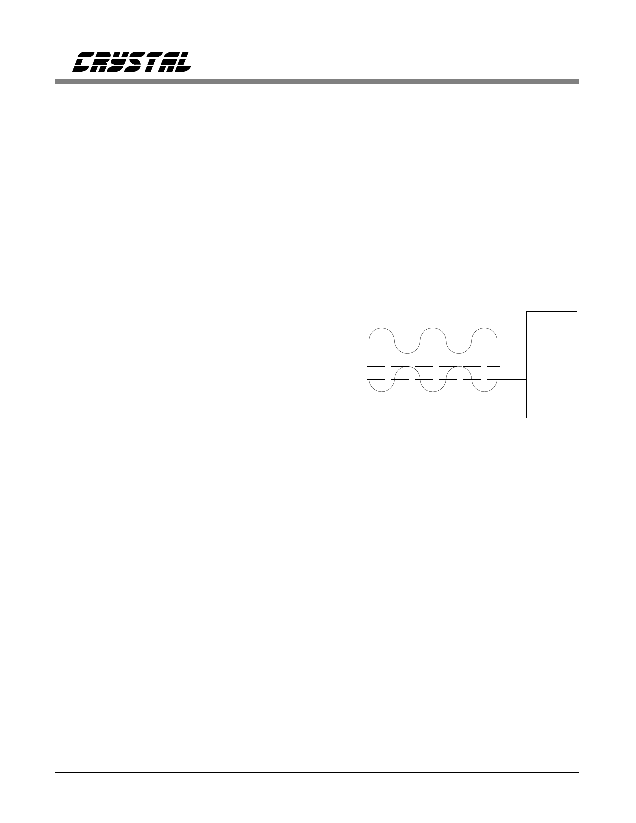
Serial Clock
The serial clock shifts the digitized audio data
from the internal data registers via the
SDATA pin. SCLK is an output in Master Mode.
Internal dividers will divide the master clock by
4 to generate a serial clock which is 64× Fs. In
Slave Mode, SCLK is an input with a serial
clock typically between 48× and 128× Fs. How-
ever, the serial clock must be a minimum of 64×
Fs to access the Peak Signal Level bits.
Left / Right Clock
The Left/Right clock determines which channel,
left or right, is to be output on SDATA. Although
the outputs for each channel are transmitted at
different times, Left/Right pairs represent simul-
taneously sampled analog inputs. In Master
Mode, LRCK is an output whose frequency is
equal to Fs. In Slave Mode, LRCK is an input
whose frequency must be equal to the output
sample rate, Fs.
Master Mode
In Master mode, SCLK and LRCK are outputs
which are internally derived from the Master
Clock. Internal dividers will divide MCLK by 4
to generate a SCLK which is 64× Fs and by 256
to generate a LRCK which is equal to Fs. Master
mode is only supported with a 256× master
clock. The CS5334/5 is placed in the Master
mode with a 47 kΩ pull-down resistor on the
OVFL pin.
Slave Mode
LRCK and SCLK become inputs in SLAVE
mode. LRCK must be externally derived from
MCLK and be equal to Fs. The serial clock is
typically between 64× and 128× Fs. A 48× Fs
serial clock is possible though will not allow ac-
cess to the Peak Signal Level bits. Master clock
frequencies of 256×, 384× and 512× Fs are sup-
ported. The ratio of the applied master clock to
the left/right clock is automatically detected dur-
ing power-up and internal dividers are set to gen-
erate the appropriate internal clocks.
Analog Connections
Figure 1 shows the analog input connections.
The analog inputs are presented to the modula-
tors via the AINR+/- and AINL+/- pins. Each
analog input pin will accept a maximum of
1 Vrms centered at +2.2 Volt as shown in Fig-
ure 6. Input signals can be AC or DC coupled
and the CMOUT output may be used as a refer-
ence for DC coupling. However, CMOUT is not
buffered and the maximum current is 10 µA.
3.6 V
2.2 V
0.78 V
3.6 V
2.2 V
0.78 V
CS5334
CS5335
AIN+
AIN-
Full Scale Input level= (AIN+) - (AIN-)= 5.67 Vpp
Figure 6. Full Scale Input Levels
The CS5334 and CS5335 sample the analog in-
puts at 128×Fs, 6.144 MHz for a 48 kHz
sample-rate. The digital filter rejects all noise
above 26.3 kHz except for frequencies right
around 6.144 MHz ± 21.7 kHz (and multiples of
6.144 MHz). Most audio signals do not have sig-
nificant energy at 6.144 MHz. Nevertheless, a
150 Ω resistor in series with each analog input
and a 2.2 nF capacitor across the inputs will at-
tenuate any noise energy at 6.144 MHz, in
addition to providing the optimum source imped-
ance for the modulators. The use of capacitors
which have a large voltage coefficient must be
avoided since these will degrade signal linearity.
NPO and COG capacitors are acceptable. If ac-
tive circuitry precedes the ADC, it is
recommended that the above RC filter is placed
between the active circuitry and the AINR and
AINL pins. The above example frequencies scale
linearly with sample rate.
DS237PP2
9
Share Link: 