CY2308SC-3 Ver la hoja de datos (PDF) - Cypress Semiconductor
Número de pieza
componentes Descripción
Lista de partido
CY2308SC-3 Datasheet PDF : 14 Pages
| |||
CY2308
Switching Characteristics for Industrial Temperature Devices (continued)
Parameter[8]
Name
Test Conditions
Min
Typ
t5
Output to Output Skew on All outputs equally loaded
–
–
same Bank (–1, –2, –3, –4)[7, 8]
Output to Output Skew
(–1H, –5H)
All outputs equally loaded
–
–
Output Bank A to Output Bank All outputs equally loaded
B Skew (–1, –4, –5H)
–
–
Output Bank A to Output Bank All outputs equally loaded
B Skew (–2, –3)
–
–
t6
Delay, REF Rising Edge to
FBK Rising Edge[78]
Measured at VDD/2
–
0
t7
Device to Device Skew[7, 8] Measured at VDD/2 on the FBK pins of
–
0
devices
t8
Output Slew Rate[7, 8]
Measured between 0.8V and 2.0V on 1
–
–1H, –5H device using Test Circuit 2
tJ
Cycle to Cycle Jitter[7, 8]
Measured at 66.67 MHz, loaded
–
75
(–1, –1H, –4, –5H)
outputs, 15 pF load
Measured at 66.67 MHz, loaded
outputs, 30 pF load
–
–
Measured at 133.3 MHz, loaded
outputs, 15 pF load
–
–
tJ
Cycle to Cycle Jitter[7, 8]
Measured at 66.67 MHz, loaded
–
–
(–2, –3)
outputs
30 pF load
tLOCK
PLL Lock Time[7, 8]
Measured at 66.67 MHz, loaded
outputs
15 pF load
Stable power supply, valid clocks
presented on REF and FBK pins
–
–
–
–
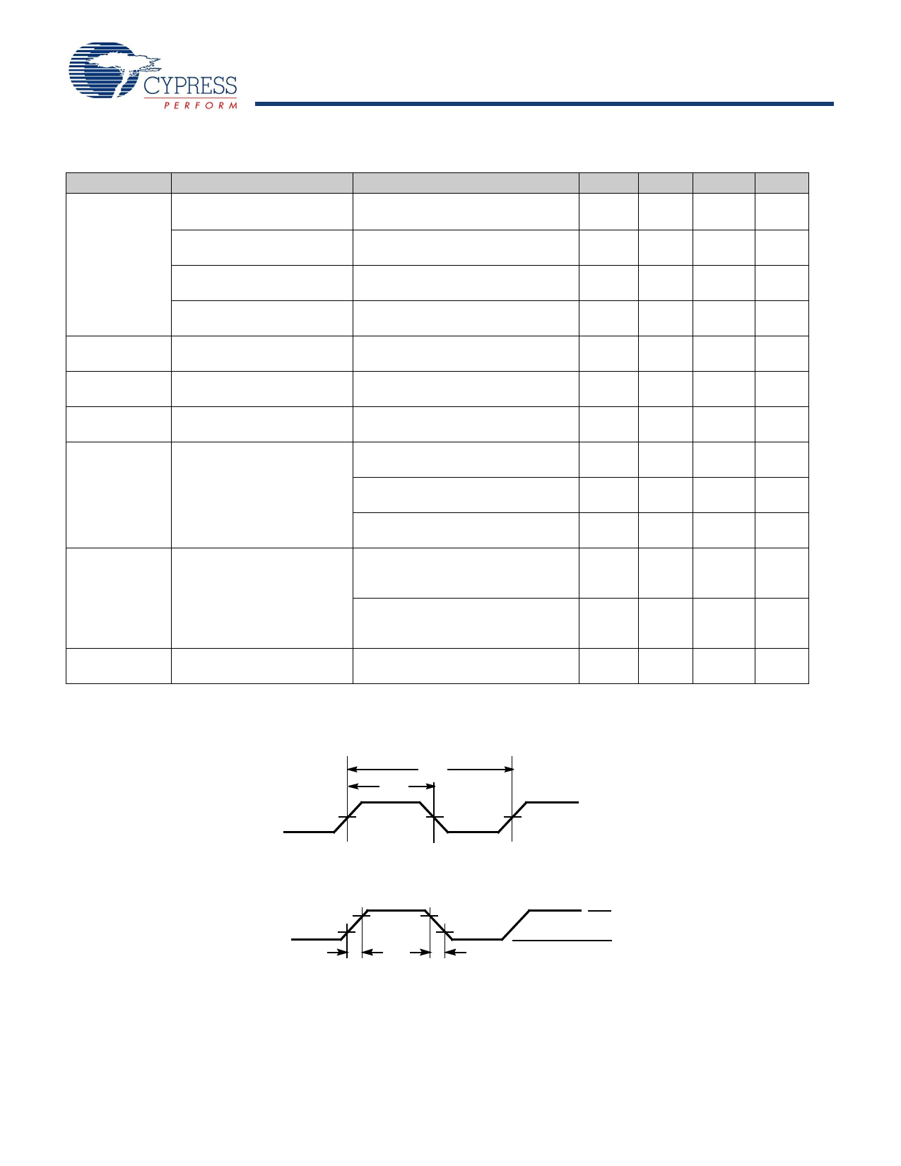
Switching Waveforms
Figure 3. Duty Cycle Timing
Max
200
200
200
400
±250
700
–
200
200
100
400
Unit
ps
ps
ps
ps
ps
ps
V/ns
ps
ps
ps
ps
400
ps
1.0
ms
1.4V
t1
t2
1.4V
1.4V
Figure 4. All Outputs Rise/Fall Time
2.0V
OUTPUT 0.8V
t3
2.0V
0.8V
t4
3.3V
0V
Document Number: 38-07146 Rev. *F
Page 7 of 14
[+] Feedback
Share Link: 