TH7107 Ver la hoja de datos (PDF) - Melexis Microelectronic Systems
Número de pieza
componentes Descripción
Lista de partido
TH7107 Datasheet PDF : 16 Pages
| |||
TH7107
315/433MHz
FSK/FM/ASK Transmitter
1 Theory of Operation
1.1 General
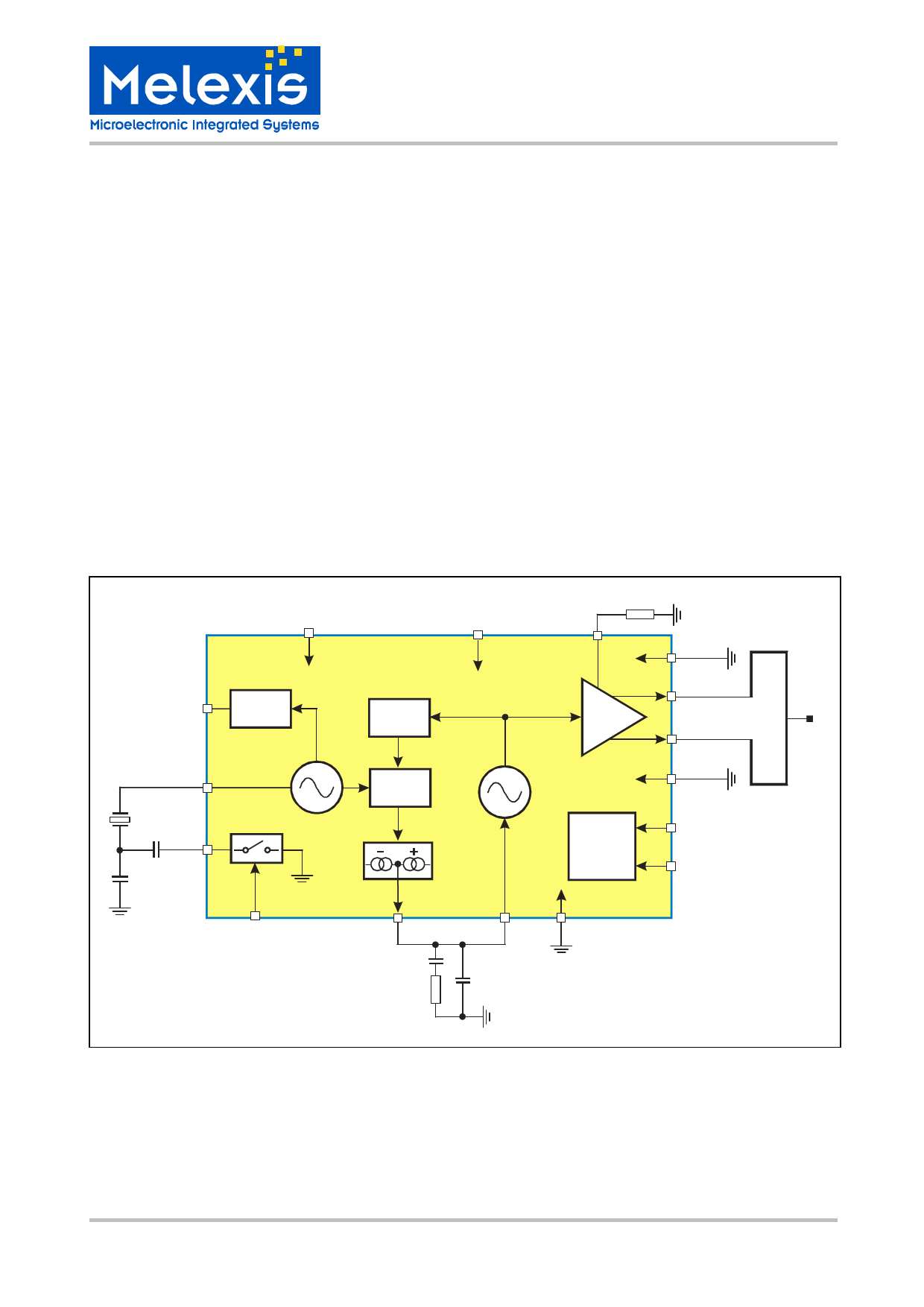
As depicted in Fig.1, the TH7107 transmitter consists of a fully integrated voltage-controlled oscillator (VCO),
a divide-by-32 divider (div32), a phase-frequency detector (PFD) and a charge pump. An external loop filter
at pin LF determines the dynamic behavior of the PLL and suppresses reference spurious signals. The
VCO’s output signal feeds the power amplifier (PA). RF signal power Po can be adjusted in six steps from
Po = –12 dBm to +2 dBm either by changing the value of resistor RPS or by varying the voltage VPS at pin
PS. The open-collector differential output (OUT1, OUT2) can be used to either directly drive a loop antenna
or to be converted to a single-ended impedance by means of a balanced-to-unbalanced (balun) transformer.
For maximum available output power, the differential output should be matched to a load of about 1 kΩ.
Bandgap biasing ensures stable operation of the IC at a power supply range of 2.2 V to 5.5 V.
1.2 Block Diagram
VCC 10
CKOUT
8
div 4
RO1
5
XTAL
RO2
CX2 4
CX1
XOSC
3 DATA
VCC 15
div32
PFD
charge
pump
RPS
PS 9
PA
VCO
mode
control
VEE
14
OUT1
13
OUT2
12
VEE
11
antenna
or
balun VCC
ENCK
7
ENTX
6
1 LF1
CF1
RF1
16 LF2 2 SUB
CF2
Fig. 1: Block diagram with external components
3901007107
Rev. 008
Page 3 of 16
Data Sheet
May/03
Share Link: 