CY7C1041BN-15ZC Ver la hoja de datos (PDF) - Cypress Semiconductor
Número de pieza
componentes Descripción
Lista de partido
CY7C1041BN-15ZC Datasheet PDF : 10 Pages
| |||
Switching Characteristics[4] Over the Operating Range (continued)
Parameter
Write Cycle[8, 9]
Description
tWC
tSCE
tAW
tHA
tSA
tPWE
tSD
tHD
tLZWE
tHZWE
tBW
Write Cycle Time
CE LOW to Write End
Address Set-Up to Write End
Address Hold from Write End
Address Set-Up to Write Start
WE Pulse Width
Data Set-Up to Write End
Data Hold from Write End
WE HIGH to Low Z[7]
WE LOW to High Z[6, 7]
Byte Enable to End of Write
-15
Min.
Max.
15
12
12
0
0
12
8
0
3
7
12
Data Retention Characteristics Over the Operating Range (L version only)
Parameter
Description
Conditions[11]
VDR
ICCDR
tCDR[3]
tR[10]
VCC for Data Retention
Data Retention Current
Chip Deselect to Data Retention Time
Operation Recovery Time
VCC = VDR = 2.0V,
CE > VCC – 0.3V,
VIN > VCC – 0.3V or VIN < 0.3V
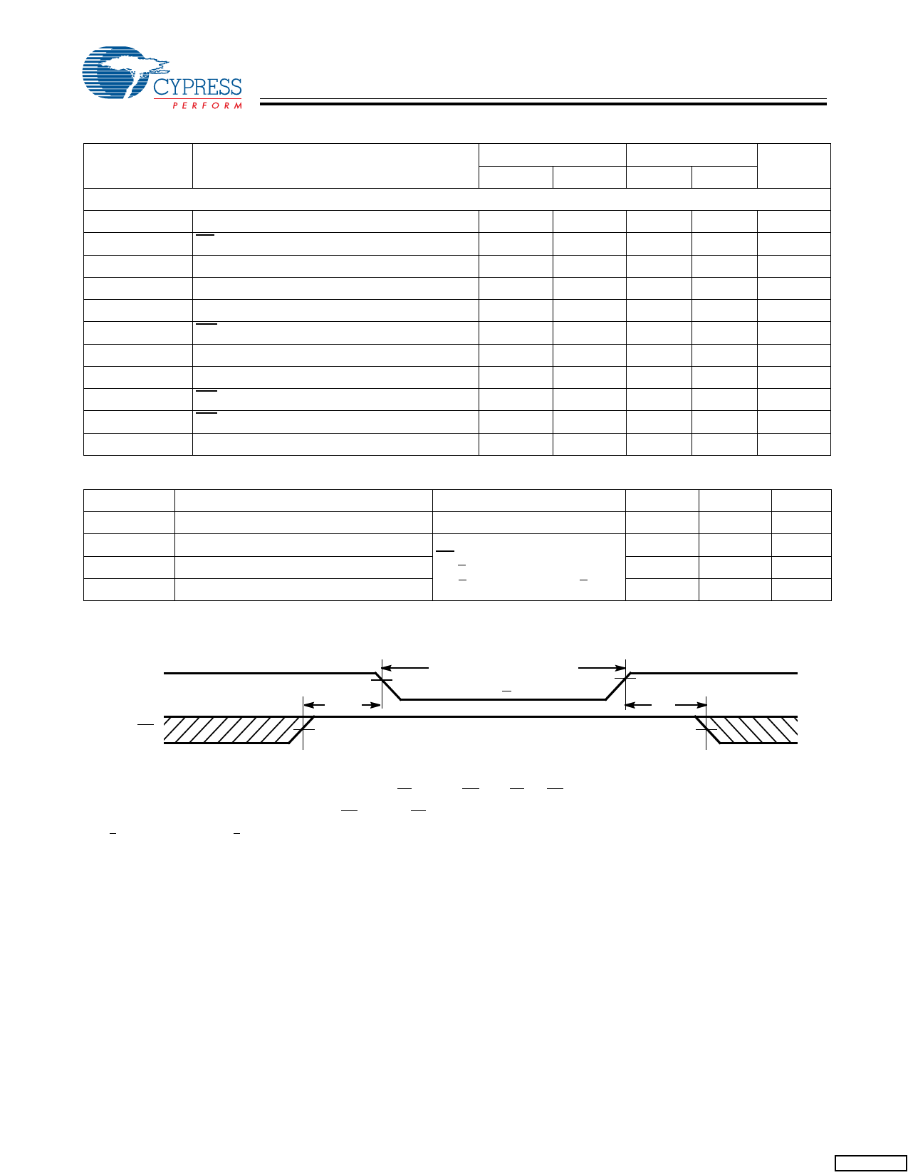
Data Retention Waveform
CY7C1041BN
-20
Min.
Max.
Unit
20
ns
13
ns
13
ns
0
ns
0
ns
13
ns
9
ns
0
ns
3
ns
8
ns
13
ns
Min.
2.0
0
tRC
Max.
Unit
V
200
µA
ns
ns
DATA RETENTION MODE
VCC
3.0V
VDR > 2V
3.0V
tCDR
tR
CE
Notes:
8. The internal write time of the memory is defined by the overlap of CE LOW, and WE LOW. CE and WE must be LOW to initiate a write, and the transition of either
of these signals can terminate the write. The input data set-up and hold timing should be referenced to the leading edge of the signal that terminates the write.
9. The minimum write cycle time for Write Cycle no. 3 (WE controlled, OE LOW) is the sum of tHZWE and tSD.
10. tr < 3 ns for the -15 speed. tr < 5 ns for the -20 and slower speeds.
11. No input may exceed VCC + 0.5V.
Document #: 001-06496 Rev. *A
Page 4 of 10
[+] Feedback
Share Link: 