CY7C4425-35AI Ver la hoja de datos (PDF) - Cypress Semiconductor
Número de pieza
componentes Descripción
Lista de partido
CY7C4425-35AI Datasheet PDF : 25 Pages
| |||
CY7C4425/4205/4215
CY7C4225/4235/4245
every valid read cycle after retransmit, previously accessed
data is read and the read pointer is incremented until it is equal
to the write pointer. Flags are governed by the relative loca-
tions of the read and write pointers and are updated during a
retransmit cycle. Data written to the FIFO after activation of RT
are transmitted also.
The full depth of the FIFO can be repeatedly retransmitted.
Table 2. Flag Truth Table.
Number of Words in FIFO
7C4425 - 64 x 18
7C4205 - 256 x 18
7C4215 - 512 x 18
0
1 to n[37
0
1 to n[37]
0
1 to n[37]
(n+1) to 32
(n+1) to 128
(n+1) to 256
33 to (64 – (m+1))
(64 – m)[38] to 63
129 to (256 – (m+1))
(256 – m)[38] to 255
257 to (512 – (m+1))
(512 – m)[38] to 511
64
256
512
FF
PAF
HF
PAE
EF
H
H
H
L
L
H
H
H
L
H
H
H
H
H
H
H
H
L
H
H
H
L
L
H
H
L
L
L
H
H
Number of Words in FIFO
7C4225 - 1K x 18
7C4235 - 2K x 18
7C4245 - 4K x 18
FF
PAF
HF
PAE
EF
0
1 to n[37]
0
1 to n[37]
0
1 to n[37]
H
H
H
L
L
H
H
H
L
H
(n+1) to 512
(n+1) to 1024
(n+1) to 2048
H
H
H
H
H
513 to (1024 – (m+1)) 1025 to (2048 – (m+1)) 2049 to (4096 – (m+1))
H
H
L
H
H
(1024 – m)[38] to 1023
(2048 – m)[38] to 2047
(4096 – m)[38] to 4095
H
L
L
H
H
1024
2048
4096
L
L
L
H
H
Notes:
37. n = Empty Offset (Default Values: CY7C4425 n = 7, CY7C4205 n = 31, CY7C4215 n = 63, CY7C4225/7C4235/7C4245 n = 127).
38. m = Full Offset (Default Values: CY7C4425 n = 7, CY7C4205 n = 31, CY7C4215 n = 63, CY7C4225/7C4235/7C4245 n = 127).
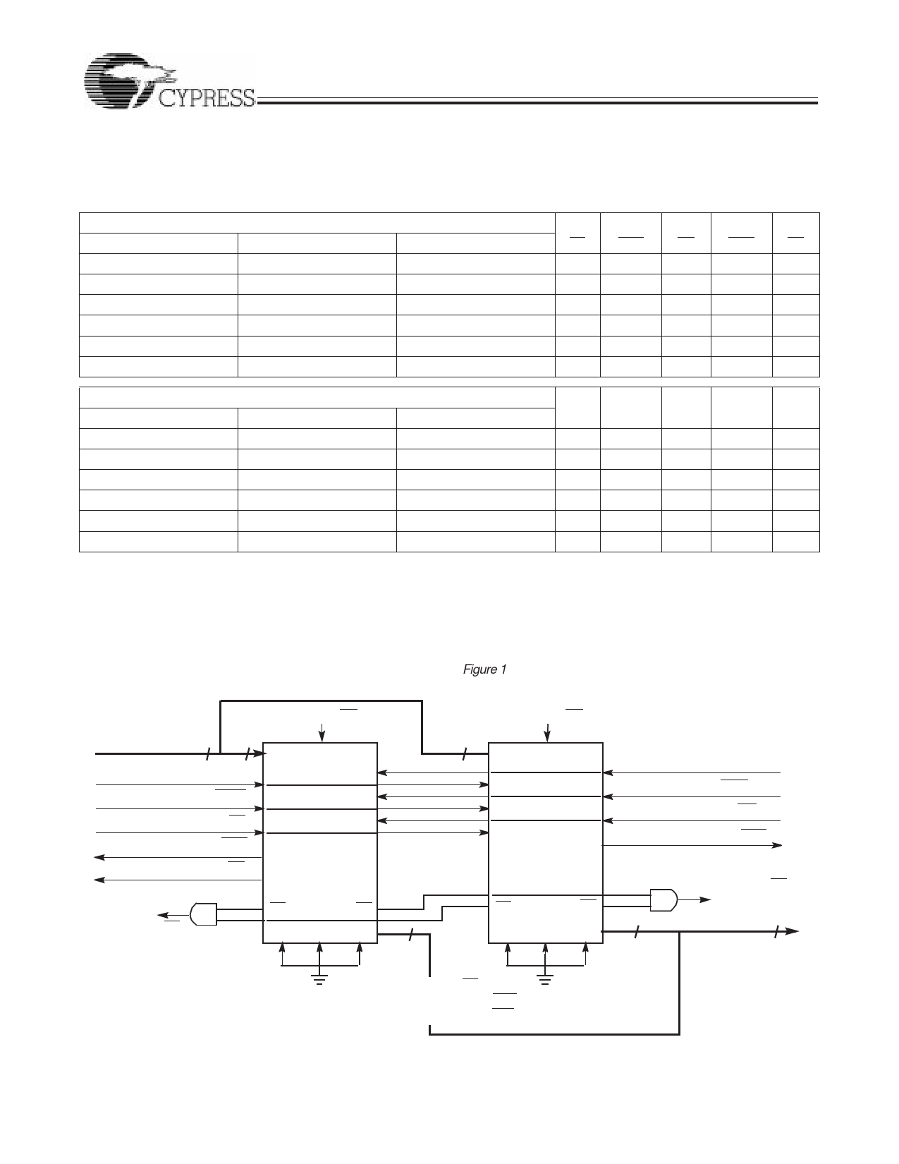
Width Expansion Configuration
The CY7C42X5 can be expanded in width to provide word
widths greater than 18 in increments of 18. During width ex-
pansion mode all control line inputs are common and all flags
are available. Empty (Full) flags should be created by ANDing
the Empty (Full) flags of every FIFO. This technique will avoid
ready data from the FIFO that is “staggered” by one clock cycle
due to the variations in skew between RCLK and WCLK.
Figure 1 demonstrates a 36-word width by using two CY7C42X5.
RESET (RS)
DATA IN (D) 36 18
WRITECLOCK (WCLK)
WRITEENABLE (WEN)
LOAD (LD)
PROGRAMMABLE(PAE)
7C4425
HALF FULL FLAG (HF)
7C4205
7C4215
7C4225
7C4235
FF 7C4235 EF
FULL FLAG (FF)
18
RESET (RS)
18
READ CLOCK (RCLK)
READ ENABLE (REN)
7C4425
7C4205
7C4215
7C4225
7C4235
7C4235
FF
EF
OUTPUTENABLE (OE)
PROGRAMMABLE(PAF)
EMPTYFLAG (EF)
18 DATA OUT (Q) 36
FIRSTLOAD (FL)
WRITE EXPANSION IN (WXI)
READ EXPANSION IN (RXI)
42X5–24
Figure 1. Block Diagram of 64x36/256 x 36/512 x 36/1024 x 36/2048 x 36/4096 x 36 Synchronous FIFO Memory Used in a
Width Expansion Configuration.
15
Share Link: 