CY7C4205V Ver la hoja de datos (PDF) - Cypress Semiconductor
Número de pieza
componentes Descripción
Lista de partido
CY7C4205V Datasheet PDF : 20 Pages
| |||
CY7C4225V/4205V/4215V
CY7C4425V/4235V/4245V
Maximum Ratings[4]
(Above which the useful life may be impaired. For user guide-
lines, not tested.)
Storage Temperature ....................................−65°C to +150°C
Ambient Temperature with
Power Applied.................................................−55°C to +125°C
Supply Voltage to Ground Potential .................−0.5V to +5.0V
DC Voltage Applied to Outputs
in High-Z State ............................................. −0.5V to VCC+0.5V
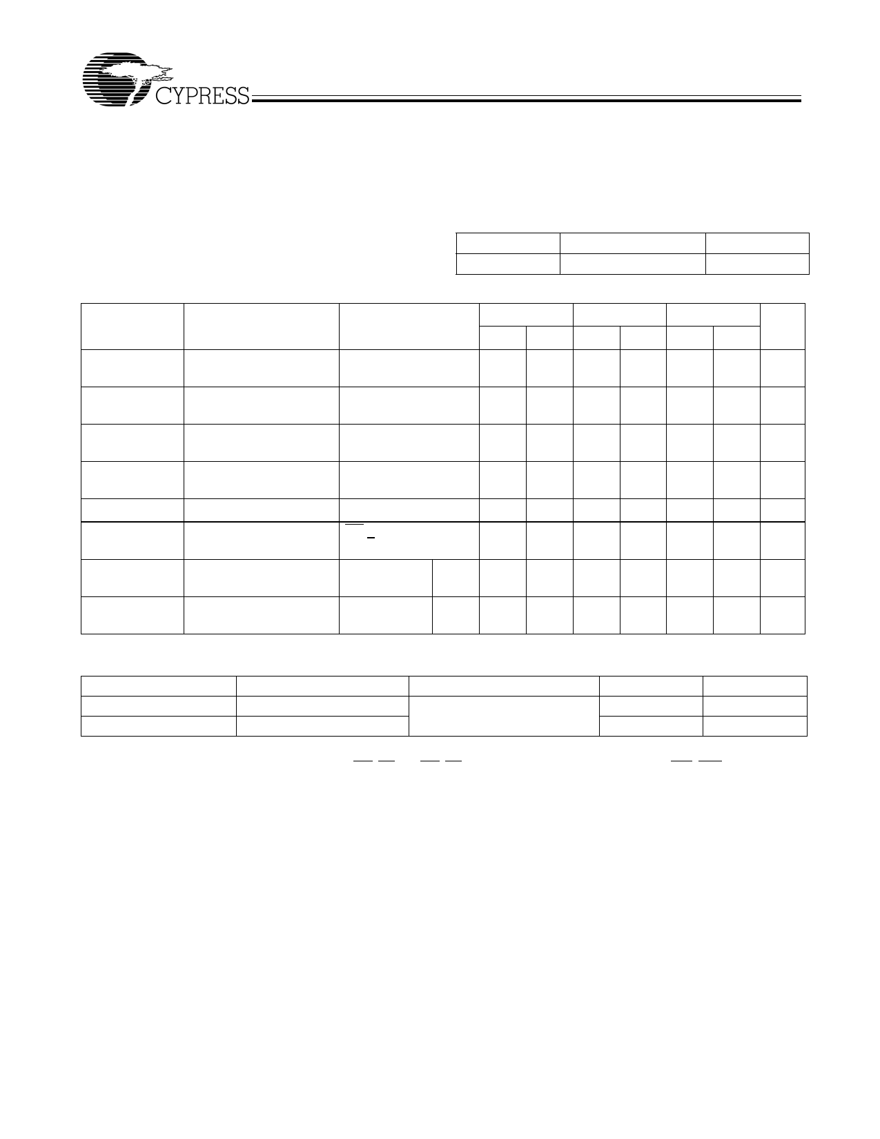
Electrical Characteristics Over the Operating Range
DC Input Voltage .................................................... −0.5V to +5V
Output Current into Outputs (LOW)............................. 20 mA
Static Discharge Voltage ........................................... >2001V
(per MIL-STD-883, Method 3015)
Latch-up Current...................................................... >200 mA
Operating Range
Range
Commercial
Ambient Temperature
VCC
0°C to +70°C
3.3V ± 300 mV
7C42X5V-15 7C42X5V-25 7C42X5V-35
Parameter
Description
Test Conditions Min. Max. Min. Max. Min. Max. Unit
VOH
VOL
VIH
VIL[5]
Output HIGH Voltage
Output LOW Voltage
Input HIGH Voltage
Input LOW Voltage
VCC = Min.,
IOH = −2.0 mA
VCC = Min.,
IOL = 8.0 mA
Low = 2.0V
High = VCC +0.5V
Low = −3.0V
High = 0.8 V
2.4
2.4
2.4
V
0.4
0.4
0.4 V
2.0 5.0 2.0 5.0 2.0 5.0 V
−0.5 0.8 −0.5 0.8 −0.5 0.8 V
IIX
IOZL
IOZH
ICC[6]
ISB[7]
Input Leakage Current VCC = Max.
−10 10 −10 10 −10 10 µA
Output OFF,
High Z Current
OE > VIH,
VSS < VO < VCC
−10 +10 −10 +10 −10 +10 µA
Operating Current
VCC = Max., Com’l
30
30
30 mA
IOUT = 0 mA
Standby Current
VCC = Max., Com’l
6
6
6 mA
IOUT = 0 mA
Capacitance[8]
Parameter
Description
Test Conditions
Max.
Unit
CIN
COUT
Input Capacitance
Output Capacitance
TA = 25°C, f = 1 MHz,
VCC = 5.0V
5
pF
7
pF
Notes:
4. The Voltage on any input or I/O pin cannot exceed the power pin during power-up
5. The VIH and VIL specifications apply for all inputs except WXI, RXI. The WXI, RXI pin is not a TTL input. It is connected to either RXO, WXO of the previous
device or VSS.
6. Input signals switch from 0V to 3V with a rise/fall time less than 3 ns, clocks and clock enables switch at 20 MHz, while the data inputs switch at 10 MHz. Outputs
are unloaded.
7. All inputs = VCC − 0.2V, except WCLK and RCLK, which are switching at 20 MHz.
8. Tested initially and after any design or process changes that may affect these parameters
Document #: 38-06029 Rev. *C
Page 8 of 20
Share Link: 