P4C163-25CM Ver la hoja de datos (PDF) - Performance Semiconductor
Número de pieza
componentes Descripción
Lista de partido
P4C163-25CM Datasheet PDF : 8 Pages
| |||
P4C163/163L
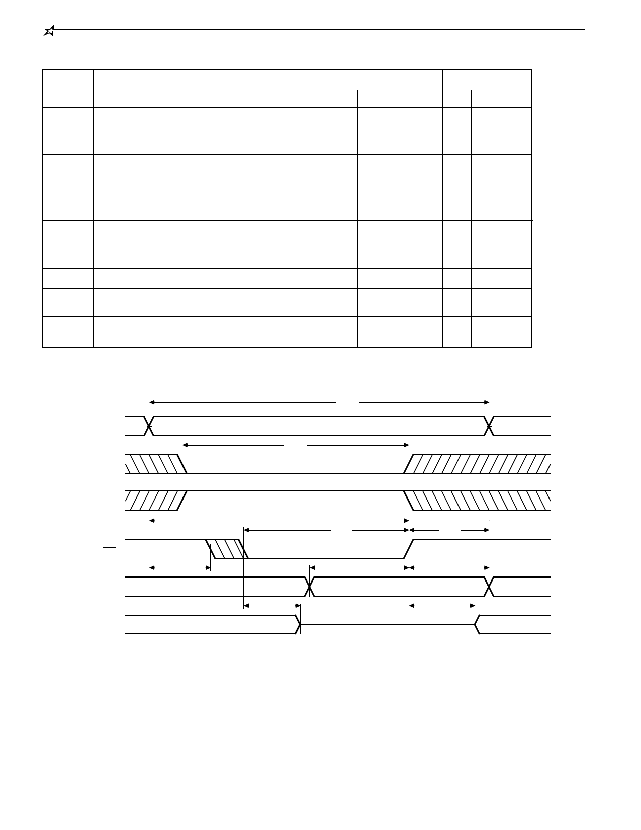
AC CHARACTERISTICS—WRITE CYCLE
(VCC = 5V ± 10%, All Temperature Ranges)(2)
Symbol
tWC
tCW
tAW
tAS
tWP
tAH
tDW
t
DH
tWZ
tOW
Parameter
Write Cycle Time
Chip Enable
Time to End of Write
Address Valid to
End of Write
Address Set-up Time
Write Pulse Width
Address Hold Time
Data Valid to End
of Write
Data Hold Time
Write Enable to
Output in High Z
Output Active
from End of Write
-25
-35
-45
Min Max Min Max Min Max Unit
25
35
45
ns
18
25
33
ns
18
25
33
ns
0
0
0
ns
18
20
25
ns
0
0
0
ns
13
15
20
ns
0
10
0
14
0
ns
18 ns
3
5
5
ns
WRITE CYCLE NO. 1 (WE CONTROLLED)(11)
ADDRESS
t CW
CE 1
(14)
t WC
CE 2
WE
DATA IN
(12)
DATA OUT
t AW
t WP
t WR
t AH
t AS
DATA UNDEFINED
t
(8)
WZ
t DW
DATA VALID
t DH
t
(8,13)
OW
HIGH IMPEDANCE
Notes:
11.
CE
1
and
WE
must
be
LOW,
and
CE2
HIGH
for
WRITE
cycle.
12. OE is LOW for this WRITE cycle to show tWZ and tOW.
13.
If
CE
1
goes
HIGH,
or
CE2
goes
LOW,
simultaneously
with
WE
HIGH,
the output remains in a low impedance state.
14. Write Cycle Time is measured from the last valid address to the first
transitioning address.
114
Share Link: 