DSP56309/D Ver la hoja de datos (PDF) - Motorola => Freescale
Número de pieza
componentes Descripción
Lista de partido
DSP56309/D Datasheet PDF : 112 Pages
| |||
Freescale Semiconductor, Inc.
Serial Communication Interface (SCI)
1.11 Serial Communication Interface (SCI)
The SCI provides a full duplex port for serial communication with other DSPs, microprocessors, or
peripherals such as modems.
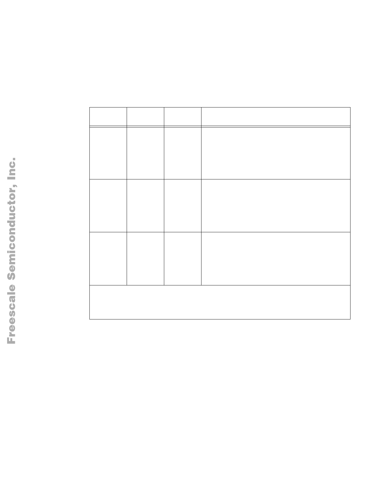
Table 1-14. Serial Communication Interface
Signal Name Type
RXD
Input
State During
Reset1,2
Signal Description
Ignored Input Serial Receive Data—Receives byte-oriented serial data and
transfers it to the SCI Receive Shift Register.
PE0
TXD
Input or Output
Output
Ignored Input
Port E 0—The default configuration following reset is GPIO input
PE0. When configured as PE0, signal direction is controlled
through the Port E Direction Register. The signal can be
configured as an SCI signal RXD through the Port E Control
Register.
Serial Transmit Data—Transmits data from the SCI Transmit
Data Register.
PE1
SCLK
Input or Output
Port E 1—The default configuration following reset is GPIO input
PE1. When configured as PE1, signal direction is controlled
through the Port E Direction Register. The signal can be
configured as an SCI signal TXD through the Port E Control
Register.
Input/Output
Ignored Input Serial Clock—Provides the input or output clock used by the
transmitter and/or the receiver.
PE2
Input or Output
Port E 2—The default configuration following reset is GPIO input
PE2. When configured as PE2, signal direction is controlled
through the Port E Direction Register. The signal can be
configured as an SCI signal SCLK through the Port E Control
Register.
Notes: 1. In the Stop state, the signal maintains the last state as follows:
• If the last state is input, the signal is an ignored input.
• If the last state is output, the signal is tri-stated.
2. The Wait processing state does not affect the signal state.
3. All inputs are 5 V tolerant.
1-16
For More Information On This Product,
Go to: www.freescale.com
Share Link: 