ML6554CU Ver la hoja de datos (PDF) - Micro Linear Corporation
Número de pieza
componentes Descripción
Lista de partido
ML6554CU Datasheet PDF : 14 Pages
| |||

FEATURING
ThermHPiaglOhD-WPiseEsriRpfoarStmiOonaPnPcaeckage
November 1999
PRELIMINARY
ML6554
3A Bus Termination Regulator
GENERAL DESCRIPTION
The ML6554 switching regulator is designed to convert
voltage supplies ranging from 2.3V to 4V into a desired
output voltage or termination voltage for various
applications. The ML6554 can be implemented to
produce regulated output voltages in two different modes.
In the default mode, when the VREF pin is open, the
ML6554 output voltage is 50% of the voltage applied to
VCCQ. The ML6554 can also be used to produce various
user-defined voltages by forcing a voltage on the VREFIN
pin. In this case, the output voltage follows the input
VREFIN voltage. The switching regulator is capable of
sourcing or sinking up to 3A of current while regulating an
output VTT voltage to within 3% or less.
The ML6554, used in conjunction with series termination
resistors, provides an excellent voltage source for active
termination schemes of high speed transmission lines as
those seen in high speed memory buses and distributed
backplane designs. The voltage output of the regulator
can be used as a termination voltage for other bus
interface standards such as SSTL, CMOS, Rambus™,
GTL+, VME, LV-CMOS, LV-TTL, and PECL.
FEATURES
s Power SOP package
s Can source and sink up to 3A, no heat sink required
s Integrated Power MOSFETs
s Generates termination voltages for SSTL-2 SDRAM,
SGRAM, or equivalent memories
s Generates termination voltages for active termination
schemes for GTL+, Rambus, VME, LV-TTL, PECL and
other high speed logic
s VREF input available for external voltage divider
s Separate voltages for VCCQ and PVDD
s Buffered VREF output
s VOUT of ±3% or less at 3A
s Minimum external components
s Shutdown for standby or suspend mode operation
s Thermal Shutdown » 130ºC
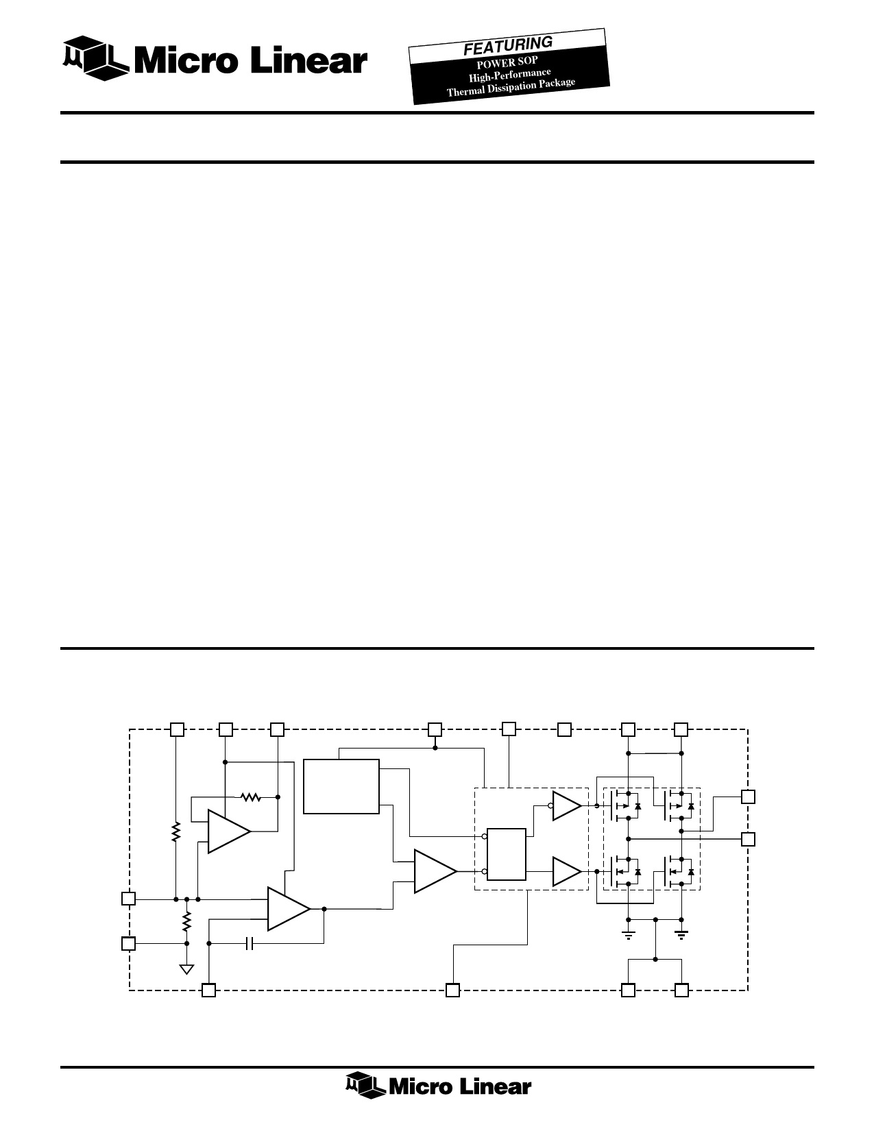
BLOCK DIAGRAM
15
16
14
VCCQ AVCC
VREFOUT
200kΩ
VREFIN
11
200kΩ
AGND
13
+
–
VREF BUFFER
OSCILLATOR/
RAMP
GENERATOR
+ ERROR AMP
–
VFB
10
1
VDD
9
VDD
12 SHDN
2
7
PVDD1 PVDD2
VL1
(VOUT)
3
SQ
–
RQ
+
RAMP
COMPARATOR
6
VL2
(VOUT)
DGND
8
PGND1 PGND2
4
5
1