RF2640 Ver la hoja de datos (PDF) - RF Micro Devices
Número de pieza
componentes Descripción
Lista de partido
RF2640 Datasheet PDF : 6 Pages
| |||
Preliminary
RF2640
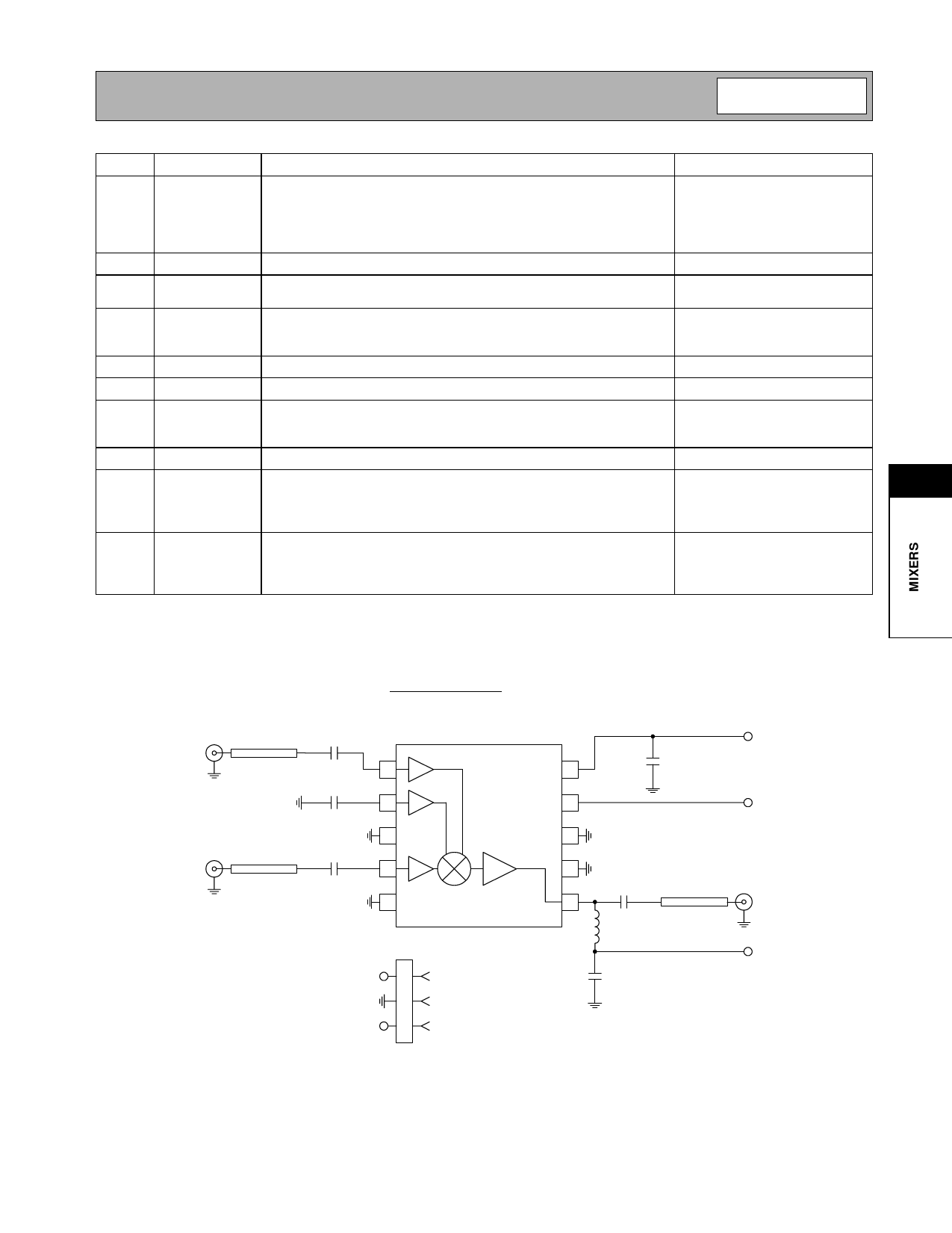
Pin Function Description
Interface Schematic
2/26/1997
1
IF+
Balanced IF input pin. This pin is internally DC-biased and should be
DC-blocked if connected to a device with a DC level present. For single-
ended input operation, one pin is used as an input and the other IF
input is AC-coupled to ground. The single-ended input impedance is
50 Ω.
2
IF-
Same as pin 1, except complementary input.
3
GND1
Ground connection. For best performance, keep traces physically short
and connect immediately to ground plane.
4
LO+
Single-ended LO input pin. This pin is internally DC-biased and should
be DC-blocked if connected to a device with a DC level present. The
single-ended input impedance is 50Ω.
5
GND2
Same as pin 3, except complementary input.
6
RF OUT RF Output Pin. The output impedance is 50Ω.
7
RF GND This pin requires a small inductance to ground to optimize the gain and
third order intercept point. See Evaluation Board Layout. The trace
length on the board is approximately 65mils.
8
GND3
Same as pin 7.
9
PD
Power down control. When logic “high” (between 1.2V and 1.8V) the
6
device is active and all circuits are operating. When logic “low”
(between 0.0V and 0.6V) the device is inactive and all circuits are
turned off.
10
VCC
Supply Voltage pin. External bypassing is required. External RF, LO,
and IF bypassing is required. The trace length between the pin and the
bypass capacitors should be minimized. The ground side of the bypass
capacitors should connect immediately to ground plane.
J1
IF IN
J2
LO IN
Evaluation Board Schematic
RF=836MHz, LO=1016MHz
(Download Bill of Materials from www.rfmd.com.)
50 Ω µstrip
C1
1 nF
C2
1
1 nF
2
C3
3
50 Ω µstrip
22 pF
4
5
P1-1
P1-3
P1
1 PD
2 GND
3 VCC
C6
10
1 nF
9
8
7
C3
22 pF
50 Ω µstrip
6
L1
12 nH
C4
1 nF
VCC
PD
J3
RF OUT
VCC
Rev A3 010717
6-39
Share Link: 