RF2466 Ver la hoja de datos (PDF) - RF Micro Devices
Número de pieza
componentes Descripción
Lista de partido
RF2466 Datasheet PDF : 8 Pages
| |||
RF2466
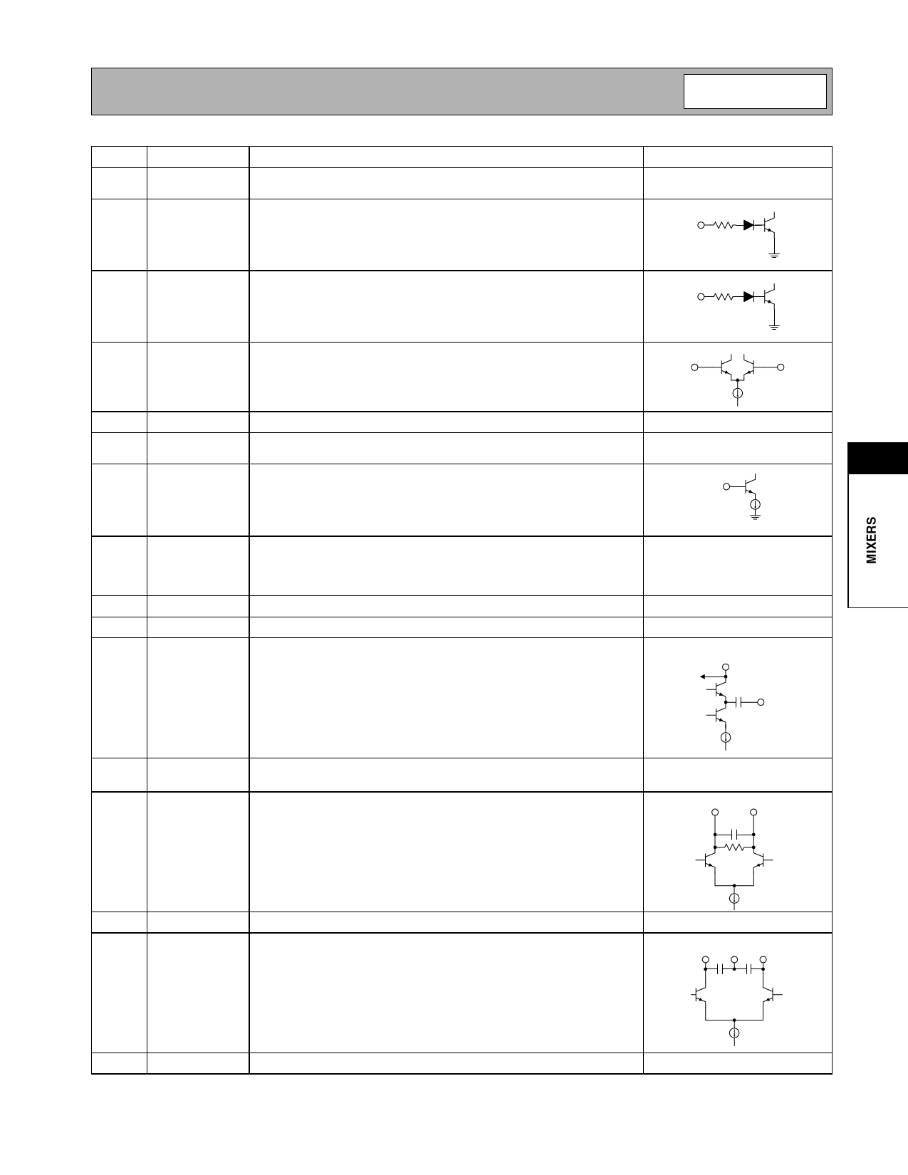
Pin Function Description
Interface Schematic
1
GND
Ground connection. For best performance, keep traces physically short
and connect immediately to ground plane.
2
IF SELECT Control line for IF out select. A logic “low” enables the FM output. A
logic “high” enables the CDMA output. The threshold voltage is 1.6V,
and the pin draws less than 50µA when selected.
50 kΩ
C1
3
PD
Power down pin. A logic “low” (<1.6V) turns the part off. A logic “high”
(>1.6V) turns the part on. In addition, pin 2 (IF SELECT) should also be
50 kΩ
PD
taken low during power down.
4
LO+
Mixer LO balanced input pin. For single-ended input operation, this pin
LO IN+
LO IN-
is used as an input and pin 5 is bypassed to ground.
5
LO-
Same as pin 4 except complementary input.
See pin 4.
6
GND
Ground connection for the mixer. For best performance, keep traces
physically short and connect immediately to ground plane.
6
7
MIXER IN Mixer RF input pin. This pin is internally DC-biased and should be DC
blocked if connected to a device with DC present. External matching
MIX IN
network sets RF and IF impedance for optimum performance.
8
BYPASS Internal voltage reference. External RF and IF bypassing is required.
The trace length between the pin and the bypass capacitors should be
minimized. The ground side of the bypass capacitors should connect
immediately to ground plane.
9
GND
Same as pin 1.
10
GND
Same as pin 1.
11
VCC
Supply voltage for the mixers, bias circuits, and control logic. External
RF and IF bypassing is required. The trace length between the pin and
the bypass capacitors should be minimized. The ground side of the
bypass capacitors should connect immediately to ground plane.
BIAS
VCC2
LO OUT
12
FM-
Same as pin 13, except complimentary output. For typical single ended See pin 13.
operation, this pin is connected directly to VCC.
13
FM+
FM IF output pin. This is a balanced output, but is typically used as a
single-ended output. The internal circuitry, in conjunction with an exter-
nal matching/bias inductor to VCC, sets the operating impedance. This
inductor is typically incorporated in the matching network between the
output and IF filter. The net output impedance, including the external
inductor, is about 870Ω at 85MHz. Because this pin is biased to VCC, a
DC blocking capacitor must be used if the IF filter input has a DC path
IF2+ IF2-
8.5 pF
2.1 kΩ
to ground. See Application Schematic.
14
GND
Same as pin 1.
15
CDMA+ CDMA IF output pin. This is a balanced output. The internal circuitry, in
conjunction with an external matching/bias inductor to VCC, sets the
operating impedance. This inductor is typically incorporated in the
matching network between the output and IF filter. The net output
impedance, including the external inductor, at 85MHz is higher than
1kΩ, even though the part is designed to drive a 1kΩ load. Because
this pin is biased to VCC, a DC blocking capacitor must be used if the IF
filter input has a DC path to ground. See Application Schematic.
IF1+ GND2 IF1-
1.2 1.2
pF pF
16
CDMA- Same as pin 15, except complementary output.
See pin 15.
Rev A7 010717
6-9
Share Link: 