RF2643PCBA Ver la hoja de datos (PDF) - RF Micro Devices
Número de pieza
componentes Descripción
Lista de partido
RF2643PCBA Datasheet PDF : 16 Pages
| |||
RF2643
Preliminary
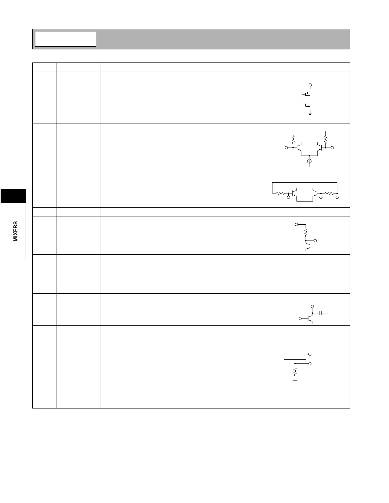
Pin Function Description
Interface Schematic
1
PD
Power Down Control. When Logic “high” (greater than 2.1V) the device
is active and all circuits are operating. When logic “low” (less than 0.5V)
VCC
the device is inactive and all circuits are turned off.
2
LO
Single-ended LO input pin. This pin is internally DC biased and should
Bias
Bias
be DC blocked if it is connected to a device with a DC level present.
The single-ended input impedance is 50Ω.
LO+
LO-
3
BYPASS Bypass pin for internal bias circuitry. Bypass with 10nF capacitor.
4
6
IF+
Balanced IF input pin. This pin is internally DC biased and should be
DC blocked if connected to a device with a DC level present. The differ-
ential input impedance is 260Ω. For single ended input operation, one
pin is used as an input and the other IF input is AC coupled to ground.
IF+
IF- Bypass
5
IF-
Same as pin 4, except complementary input.
6
PCS
RF mixer output pin for the PCS system. PCS Mixout output imped-
MIXOUT
ance depends on the LC match and it is influenced by the bypass
capacitor at VCC2.
VCC MIX
PCS MIXOUT
7
VCC MIX Supply voltage pin for the mixer. External bypassing is required. The
trace length between the pin and the bypass capacitors should be min-
imized. The ground side of the bypass capacitors should connect
immediately to ground plane.
8
VCC
Supply voltage pin for all the control and bias circuitry. A bias choke
inductor and RF bypass capacitor is required.
9
PCS VCC Supply voltage pin for the PCS driver. This pin is an open collector and
it will need a bias choke inductor and RF bypass. A parallel resistor to
the inductor improves stability of the driver amplifier.
10
PCS IN Single-ended input for the PCS driver and attenuator. External match-
ing is required. This pin is internally DC biased and should be DC
blocked if it is connected to a device with a DC level present.
11
PCS
PCS attenuator ground pin. This pin should be AC ground. The trace
ATT GND
length between the pin and the bypass capacitors should be minimized.
The value of the capacitor is chosen to resonate in the PCS band.
PCS VCC
PCS IN
PCS
Attenuator
PCS OUT
PCS ATT-GND
12
PCS OUT PCS RF output pin. External matching is required. This pin is internally
DC biased and should be DC blocked if it is connected to a device with
a DC level present.
6-40
Rev A1 010717
Share Link: 