RF2196 Ver la hoja de datos (PDF) - RF Micro Devices
Número de pieza
componentes Descripción
Lista de partido
RF2196 Datasheet PDF : 8 Pages
| |||
RF2196
Preliminary
Pin Function Description
Interface Schematic
1
GND
This pin is internally grounded to the die flag.
2
VREG1 Power Down control for first stage. Regulated voltage supply for ampli-
fier bias. In Power Down mode, both VREG and VMODE need to be LOW
(< 0.5 V).
3
MODE
For nominal operation (High Gain Mode), VMODE is set LOW. When set
2
HIGH, the driver and final are dynamically scaled to reduce the device
size and as a result to reduce idle current.
4
VREG2 Power Down control for the second stage. Regulated voltage supply for
amplifier bias. In Power Down mode, both VREG and VMODE need to be
LOW (<0.5V).
5
GND
Connect to ground plane via 15nH inductor. DC return for the second
stage bias circuit.
6
NC
This pin has no internal bonding; therefore, this pin can be connected
to output pin 7, connected to the ground plane, or not connected. Slight
tuning of the output match may be required due to stray capacitance of
the pin.
7
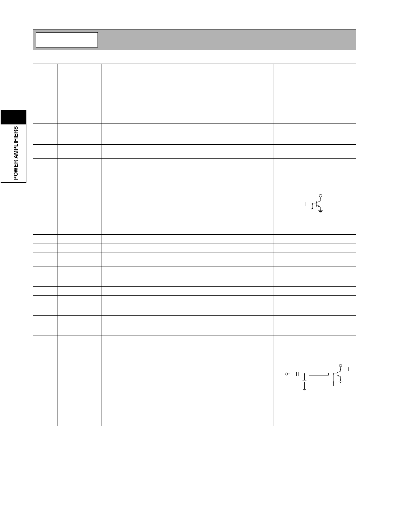
RF OUT RF output and power supply for final stage. This is the unmatched col-
lector output of the second stage. A DC block is required following the
matching components. The biasing may be provided via a parallel L-C
set for resonance at the operating frequency of 1710MHz to 1910MHz.
It is important to select an inductor with very low DC resistance with a
1A current rating. Alternatively, shunt microstrip techniques are also
applicable and provide very low DC resistance. Low frequency bypass-
ing is required for stability.
RF OUT
From Bias
Network
8
RF OUT Same as pin 7.
See pin 7.
9
GND
This pin is internally grounded to the die flag.
10
VCC
Supply for bias reference and control circuits. High frequency bypass-
ing may be necessary.
11
VCC1
Power supply for first stage and interstage match. Pins 11 and 12
should be connected by a common trace where the pins contact the
printed circuit board.
12
VCC1
Same as pin 11.
13
NC
It is recommended that these pins be connected to the ground plane for
improved isolation between RF IN (pin 16) and the VCC1 pins (pins 11
and 12).
14
NC
It is recommended that these pins be connected to the ground plane for
improved isolation between RF IN (pin 16) and the VCC1 pins (pins 11
and 12).
15
NC
It is recommended that these pins be connected to the ground plane for
improved isolation between RF IN (pin 16) and the VCC1 pins (pins 11
and 12).
16
RF IN
RF input. An external 15pF series capacitor is required as a DC block.
VCC1
In addition, the matching circuit shown is required to improve input
VSWR.
15 pF
TL
RF IN
3.6 pF
GND1
From
Bias
Stages
Pkg
Base
GND
Ground connection. The backside of the package should be soldered to
a top side ground pad which is connected to the ground plane with mul-
tiple vias. The pad should have a short thermal path to the ground
plane.
2-206
Rev A0 010518
Share Link: 