EPA3571G Ver la hoja de datos (PDF) - PCA ELECTRONICS INC.
Número de pieza
componentes Descripción
Lista de partido
EPA3571G Datasheet PDF : 14 Pages
| |||
White Electronic Designs
WSF512K32-XXX
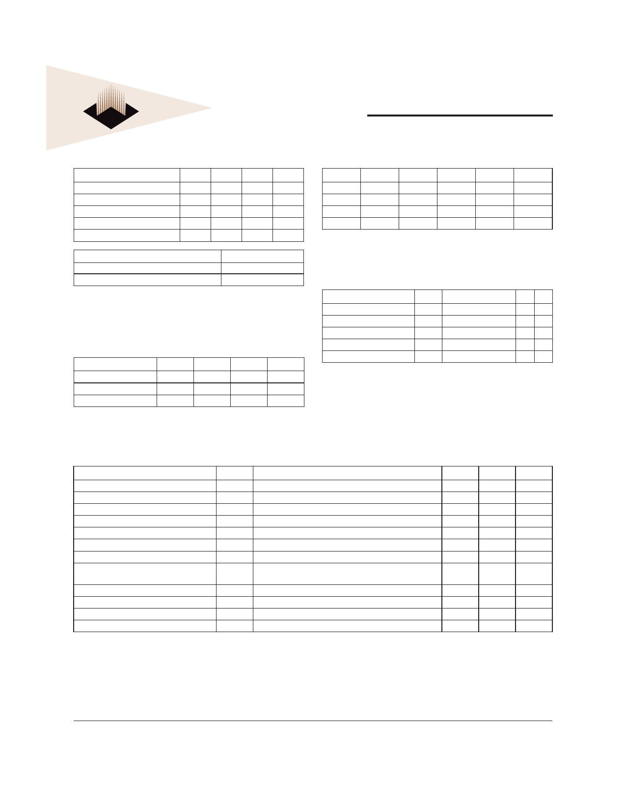
ABSOLUTE MAXIMUM RATINGS
Parameter
Symbol Min Max Unit
Operating Temperature
TA
-55 +125 °C
Storage Temperature
TSTG -65 +150 °C
Signal Voltage Relative to GND
VG
-0.5
7.0
V
Junction Temperature
TJ
150
°C
Supply Voltage
VCC
-0.5
7.0
V
Parameter
Flash Data Retention
Flash Endurance (write/erase cycles)
20 years
100,000
NOTE:
1. Stresses above the absolute maximum rating may cause permanent damage to the
device. Extended operation at the maximum levels may degrade performance and
affect reliability.
RECOMMENDED OPERATING CONDITIONS
Parameter
Supply Voltage
Input High Voltage
Input Low Voltage
Symbol
VCC
VIH
VIL
Min
Max
Unit
4.5
5.5
V
2.2 VCC + 0.3
V
-0.5
+0.8
V
SRAM TRUTH TABLE
SCS#
OE#
SWE# Mode
H
X
X
Standby
L
L
H
Read
L
H
H
Read
L
X
L
Write
NOTE:
1. FCS# must remain high when SCS# is low.
Data I/O
High Z
Data Out
High Z
Data In
Power
Standby
Active
Active
Active
CAPACITANCE
Ta = +25°C
Parameter
Symbol
Conditions
Max Unit
OE# capacitance
COE VIN = 0 V, f = 1.0 MHz 80 pF
F/S WE1-4# capacitance
F/S CS# capacitance
D0-31 capacitance
CWE VIN = 0 V, f = 1.0 MHz 30 pF
CCS VIN = 0 V, f = 1.0 MHz 50 pF
CI/O VI/O = 0 V, f = 1.0 MHz 30 pF
A0-18 capacitance
CAD VIN = 0 V, f = 1.0 MHz 80 pF
This parameter is guaranteed by design but not tested.
DC CHARACTERISTICS
VCC = 5.0V, VSS = 0V, -55°C ≤ TA ≤ +125°C
Parameter
Input Leakage Current
Output Leakage Current
SRAM Operating Supply Current x 32 Mode
Standby Current
SRAM Output Low Voltage
SRAM Output High Voltage
Flash VCC Active Current for Read (1)
Flash VCC Active Current for Program or
Erase (2)
Flash Output Low Voltage
Flash Output High Voltage
Flash Output High Voltage
Flash Low VCC Lock Out Voltage
Symbol
ILI
ILO
ICCx32
ISB
VOL
VOH
ICC1
ICC2
Conditions
VCC = 5.5, VIN = GND to VCC
SCS# = VIH, OE# = VIH, VOUT = GND to VCC
SCS# = VIL, OE# = FCS# = VIH, f = 5MHz, VCC = 5.5
FCS# = SCS# = VIH, OE# = VIH, f = 5MHz, VCC = 5.5
IOL = 6mA, VCC = 4.5
IOH = -4.0mA, VCC = 4.5
FCS# = VIL, OE# = SCS# = VIH
FCS# = VIL, OE# = SCS# = VIH
VOL IOL = 8.0mA, VCC = 4.5
VOH1 IOH = -2.5 mA, VCC = 4.5
VOH2 IOH = -100 µA, VCC = 4.5
VLKO
NOTES:
1. The ICC current listed includes both the DC operating current and the frequency dependent component (@ 5 MHz).
The frequency component typically is less than 2mA/MHz, with OE# at VIH.
2. ICC active while Embedded Algorithm (program or erase) is in progress.
3. DC test conditions: VIL = 0.3V, VIH = VCC - 0.3V
Min
Max
Unit
10
µA
10
µA
550
mA
90
mA
0.4
V
2.4
V
250
mA
300
mA
0.45
V
0.85 x VCC
V
VCC -0.4
V
3.2
4.2
V
May 2006
Rev. 9
3
White Electronic Designs Corporation • (602) 437-1520 • www.wedc.com
Share Link: 