LTC1598LIG(RevA) Ver la hoja de datos (PDF) - Linear Technology
Número de pieza
componentes Descripción
Lista de partido
LTC1598LIG
(Rev.:RevA)
(Rev.:RevA)
Linear Technology

LTC1598LIG Datasheet PDF : 24 Pages
| |||
LTC1594L/LTC1598L
PIN FUNCTIONS
VCC (Pin 15): Power Supply Voltage. This pin provides
power to the A/D Converter. It must be bypassed directly
to the analog ground plane.
VREF (Pin 16): Reference Input. The reference input
defines the span of the ADC.
ADCIN (Pin 17): ADC Input. This input is the positive
analog input to the ADC. Connect this pin to MUXOUT for
normal operation.
MUXOUT (Pin 18): MUX Output. This pin is the output of
the multiplexer. Tie to ADCIN for normal operation.
VCC (Pin 19): Power Supply Voltage. This pin should be
tied to Pin 15.
CH0 (Pin 20): Analog Multiplexer Input.
CH1 (Pin 21): Analog Multiplexer Input.
CH2 (Pin 22): Analog Multiplexer Input.
CH3 (Pin 23): Analog Multiplexer Input.
CH4 (Pin 24): Analog Multiplexer Input.
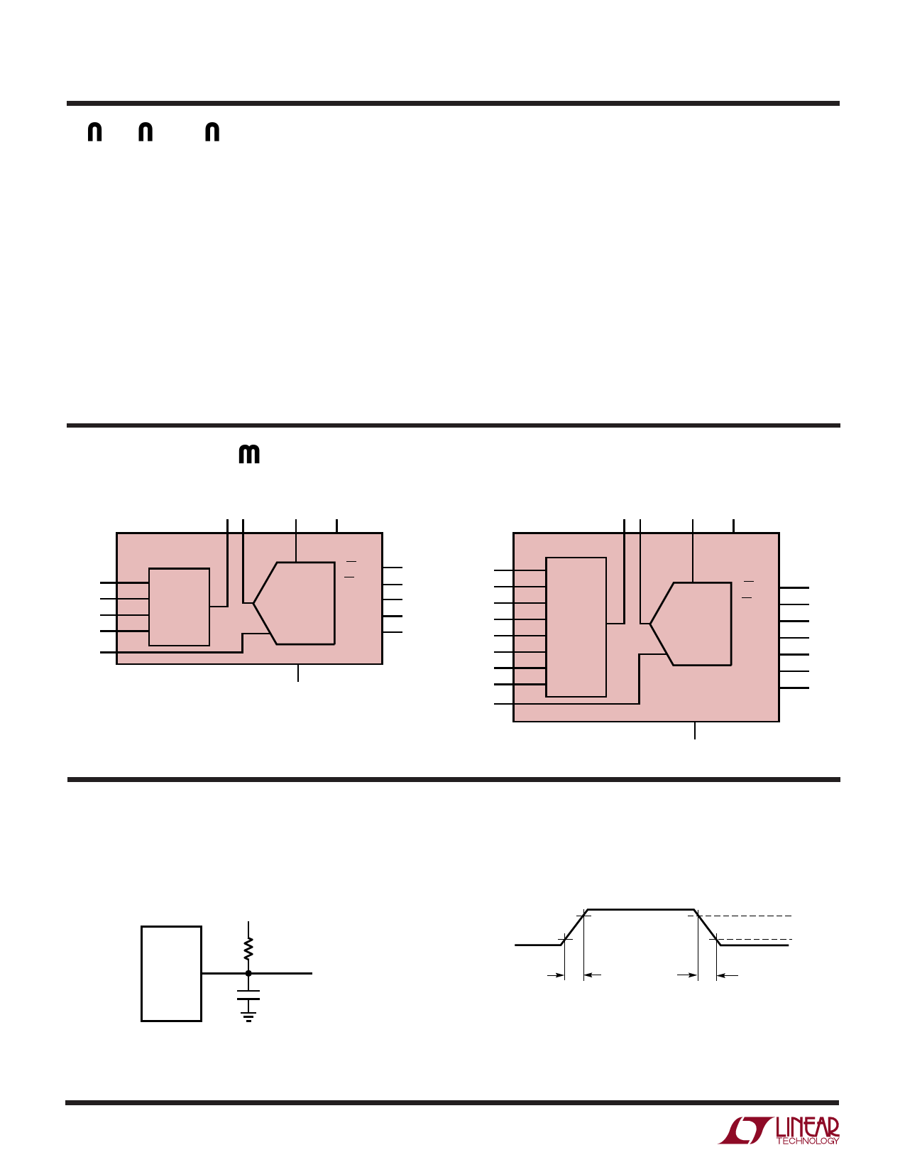
BLOCK DIAGRA S
LTC1594L
LTC1594L
15
MUXOUT
1 CH0
2 CH1
3 CH2
4 CH3
4-CHANNEL
MUX
7 COM
5
6
16
ADCIN
VREF VCC
12-BIT
+ SAMPLING
ADC
–
CSADC 9
CSMUX 13
CLK 12
DIN 14
DOUT 10
GND
8
1594L BD
LTC1598L
LTC1598L
18
MUXOUT
20 CH0
21 CH1
22 CH2
23 CH3
24 CH4
1 CH5
2 CH6
3 CH7
8-CHANNEL
MUX
8 COM
17
ADCIN
16
15, 19
VREF VCC
12-BIT
+ SAMPLING
ADC
–
GND
4, 9
CSADC
CSMUX
CLK
DIN
DOUT
NC
NC
10
6
5, 14
7
11
12
13
1598L BD
TEST CIRCUITS
Load Circuit for tdDO, tr and tf
DOUT
1.4V
3k
100pF
TEST POINT
1594L/98L TC01
Voltage Waveforms for DOUT Rise and Fall Times, tr, tf
DOUT
tr
VOH
VOL
tf
1594L/98L TC02
8
Share Link: