FM200TU-3A Ver la hoja de datos (PDF) - Mitsumi
Número de pieza
componentes Descripción
Lista de partido
FM200TU-3A Datasheet PDF : 5 Pages
| |||
MITSUBISHI <MOSFET MODULE>
FM200TU-3A
HIGH POWER SWITCHING USE
INSULATED PACKAGE
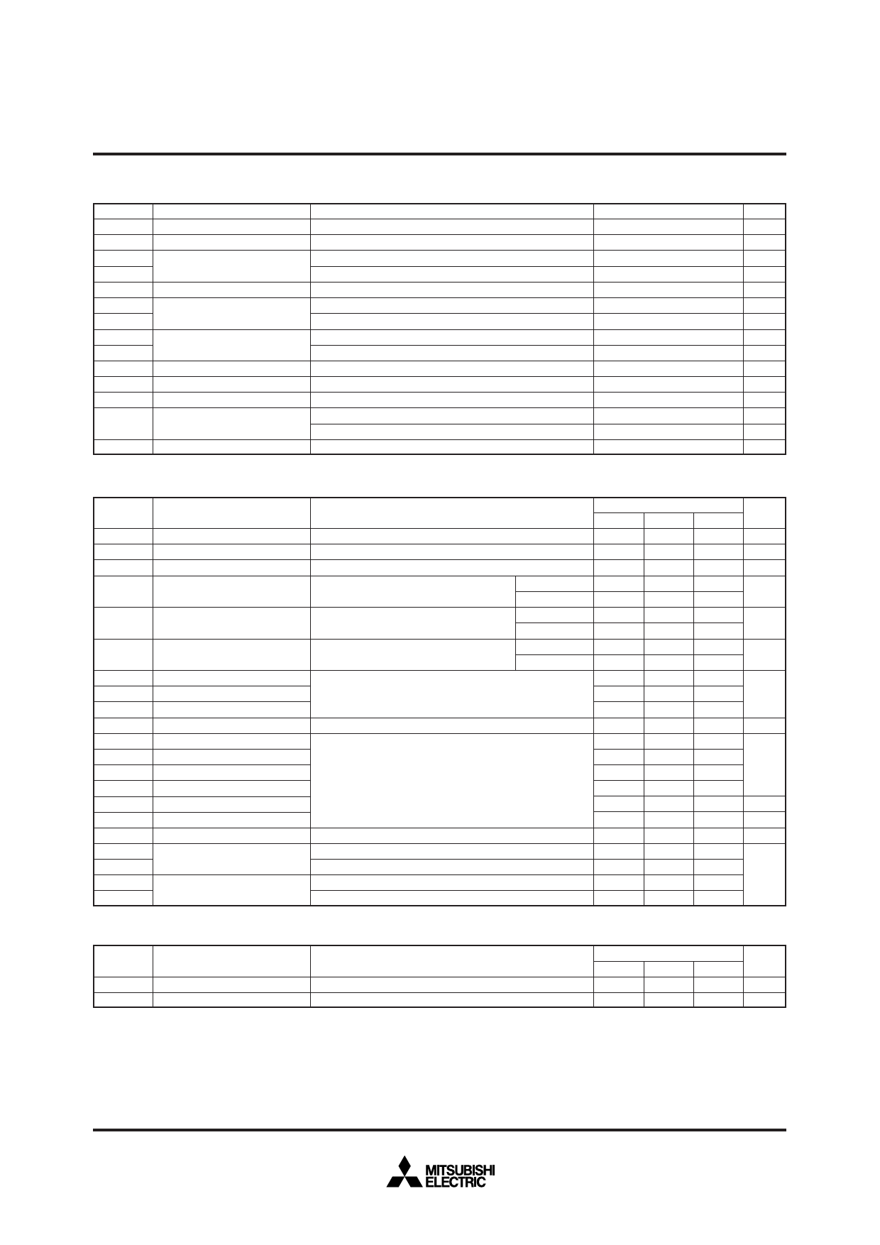
ABSOLUTE MAXIMUM RATINGS (Tch = 25°C unless otherwise specified.)
Symbol
VDSS
VGSS
ID
IDM
IDA
IS*1
ISM*1
PD*4
PD*4
Tch
Tstg
Viso
Item
Drain-source voltage
Gate-source voltage
Drain current
Avalanche current
Source current
Maximum power dissipation
Channel temperature
Storage temperature
Isolation voltage
—
Mounting torque
—
Weight
G-S Short
D-S Short
TC’ = 122°C*3
Pulse*2
L = 10µH Pulse*2
Conditions
Pulse*2
TC = 25°C
TC’ = 25°C*3
Main terminal to base plate, AC 1 min.
Main Terminal M6
Mounting M6
Typical value
Ratings
150
±20
100
200
100
100
200
410
560
–40 ~ +150
–40 ~ +125
2500
3.5 ~ 4.5
3.5 ~ 4.5
600
Unit
V
V
A
A
A
A
A
W
W
°C
°C
V
N•m
N•m
g
ELECTRICAL CHARACTERISTICS (Tch = 25°C unless otherwise specified.)
Symbol
Item
Conditions
IDSS
VGS(th)
IGSS
rDS(ON)
(chip)
VDS(ON)
(chip)
R(lead)
Ciss
Coss
Crss
QG
td(on)
tr
td(off)
tf
trr*1
Qrr*1
VSD*1
Rth(ch-c)
Rth(ch-c’)
Rth(c-f)
Rth(c’-f’)
Drain cutoff current
Gate-source threshold voltage
Gate leakage current
Static drain-source
On-state resistance
Static drain-source
On-state voltage
Lead resistance
Input capacitance
Output capacitance
Reverse transfer capacitance
Total gate charge
Turn-on delay time
Turn-on rise time
Turn-off delay time
Turn-off fall time
Reverse recovery time
Reverse recovery charge
Source-drain voltage
Thermal resistance
Contact thermal resistance
VDS = VDSS, VGS = 0V
ID = 10mA, VDS = 10V
VGS = VGSS, VDS = 0V
ID = 100A
VGS = 15V
ID = 100A
VGS = 15V
ID = 100A
terminal-chip
VDS = 10V
VGS = 0V
VDD = 80V, ID = 100A, VGS = 15V
Tch = 25°C
Tch = 125°C
Tch = 25°C
Tch = 125°C
Tch = 25°C
Tch = 125°C
VDD = 80V, ID = 100A, VGS1 = VGS2 = 15V
RG = 13Ω, Inductive load switching operation
IS = 100A
IS = 100A, VGS = 0V
MOSFET part (1/6 module)*7
MOSFET part (1/6 module)*3
Case to fin, Thermal grease Applied*8 (1/6 module)
Case to fin, Thermal grease Applied*3, *8 (1/6 module)
Limits
Min.
Typ.
Max. Unit
—
—
1
mA
4.7
6
7.3
V
—
—
1.5
µA
—
4.8
6.6
—
9.1
—
mΩ
—
0.48
0.66
V
—
0.91
—
—
1.2
—
—
1.68
—
mΩ
—
—
50
—
—
7
nF
—
—
4
—
820
—
nC
—
—
400
—
—
250
ns
—
—
450
—
—
200
—
—
200
ns
—
6.5
—
µC
—
—
1.3
V
—
—
0.30
—
—
0.22
—
0.1
—
°C/W
—
0.09
—
THERMISTOR PART
Symbol
Parameter
Conditions
Limits
Unit
Min.
Typ.
Max.
RTH*6
B*6
Resistance
B Constant
TTH = 25°C*5
Resistance at TTH = 25°C, 50°C*5
—
100
—
kΩ
—
4000
—
K
*1: It is characteristics of the anti-parallel, source to drain free-wheel diode (FWDi).
*2: Pulse width and repetition rate should be such that the device channel temperature (Tch) does not exceed Tch max rating.
*3: TC’ measured point is just under the chips. If use this value, Rth(f-a) should be measured just under the chips.
*4: Pulse width and repetition rate should be such as to cause negligible temperature rise.
*5: TTH is thermistor temperature.
*6: B = (InR1-InR2)/(1/T1-1/T2) R1: Resistance at T1(K), R2: Resistance at T2(K)
*7: TC measured point is shown in page OUTLINE DRAWING.
*8: Typical value is measured by using Shin-Etsu Chemical Co., Ltd “G-746”.
May 2006
Share Link: 