G5E1286 Ver la hoja de datos (PDF) - GTM CORPORATION
Número de pieza
componentes Descripción
Lista de partido
G5E1286 Datasheet PDF : 4 Pages
| |||
ISSUED DATE :2005/07/11
REVISED DATE :2006/03/29B
Functional Description
Introduction
The G5E1286 regulator is 5-terminal device designed specifically to provide extremely low dropout voltage comparable to
the PNP type without the disadvantage of the extra power dissipation due to the base current associated with PNP
regulators. This is done by bringing out the control pin of the regulator that provides the base current to the power NPN and
connecting it to a voltage that is greater than the voltage present at the Vin pin. This flexibility makes the G5E1286 ideal for
applications where dual inputs are available such as a computer motherboard with an ATX style power supply that provides
5V and 3.3V to the board. One such application is the new graphic chip sets that require anywhere from 2.4V to 2.7V
supply. The G5E1286-ADJ can easily be programmed with the addition of two external resistors to any voltages within the
range of 1.25V to 15.5V. Another major requirement of these graphic chips is the need to switch the load current from zero
to several amps in tens of nanoseconds at the processor pins, which translates to an approximately 300 to 500ns of current
step at the regulator. In addition, the output voltage tolerances are also extremely tight and they include the transient
response as part of the specification.
The G5E1286 is specifically designed to meet the fast current transient needs as well as providing an accurate initial
voltage, reducing the overall system cost with the need for fewer number of output capacitors. Another feature of the device
is its true remote sensing capability that allows accurate voltage setting at the load rather than at the device.
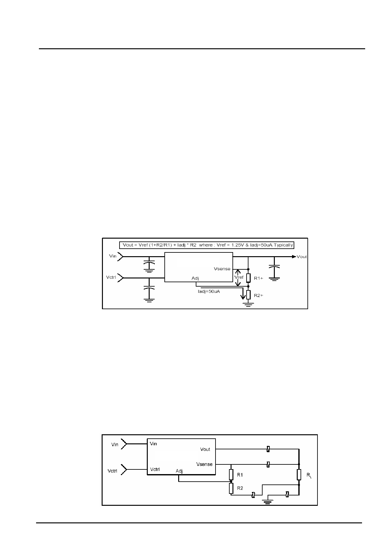
Output Voltage Setting
The G5E1286-ADJ can be programmed to any voltage in the range of 1.25V to 15.5V with the addition of R1 and R2
external resistors according to the following formula:
G5E1286-ADJ
The G5E1286-ADJ keeps a constant 1.25V between the Vsense pin and the Adj pin. By placing a resistor R1 across these
two pins and connecting the Vsense and Vout pin together, a constant current flows through R1, adding to the Iadj current
and into the R2 resistor producing a voltage equal to the (1.25/R1)*R2+Iadj*R2. This voltage is then added to the 1.25V to
set the output voltage. This is summarized in the above equation.
Since the minimum load current requirement of the G5E1286-ADJ is 10mA, R1 is typically selected to be 121 resistor so
that it automatically satisfies this condition. Notice that since Iadj is typically in the range of 50uA it only adds a small error
to the output voltage and should only be considered when a very precise output voltage setting is required.
Load Regulation
Since the G5E1286 has separate pins for the output (Vout) and the sense (Vsense), it is ideal for providing true remote
sensing of output voltage at the load. This means that the voltage drops due to parasitic resistance such PCB traces
between the regulator and the load are compensated for using remote sensing. Figure following shows a typical application
of the G5E1286-ADJ with remote sensing.
G5E1286-ADJ
G5E1286
Page: 3/4
Share Link: 