SP5748/KG/MP1S Ver la hoja de datos (PDF) - Mitel Networks
Número de pieza
componentes Descripción
Lista de partido
SP5748/KG/MP1S Datasheet PDF : 15 Pages
| |||
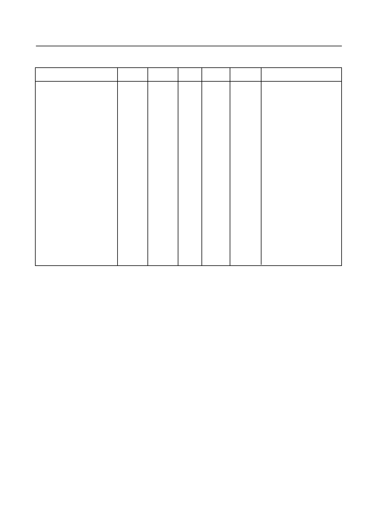
ABSOLUTE MAXIMUM RATINGS
All voltages are referred to VEE at 0V
Characteristic
Pin
Min
Supply voltage, Vcc
10
-0.3
RF input voltage
11,12
RF input DC offset
11,12
-0.3
Port voltage
7,8
-0.3
Charge pump DC offset
1
-0.3
Varactor drive DC offset
14
-0.3
Crystal DC offset
2,3
-0.3
Buffered ref output
9
-0.3
Data, clock & enable
DC offset
5,6,4
-0.3
Storage temperature
-55
Junction temperature
MP14 thermal resistance,
chip to ambient
chip to case
Power consumption at
Vcc=5.5V
ESD protection
2
SP5748 Advance Information
Typ
Max
Units
Conditions
7
V
2.5
Vcc+0.3
Vcc+0.3
Vcc+0.3
Vcc+0.3
Vcc+0.3
Vcc+0.3
Vcc+0.3
Vp-p
V
V
V
V
V
V
V
Differential across pins
11 and 12
+125
°C
+150
°C
81
27
TBC
°C/W
°C/W
mW
All ports off
kV Mil-std 883B latest revision
method 3015 cat.1.
Functional description
The SP5748 contains all the elements necessary, with
the exception of a frequency reference, loop filter and
external high voltage transistor, to control a varicap
tuned local oscillator, so forming a complete PLL
frequency synthesised source. The device allows for
operation with a high comparison frequency and is
fabricated in high speed logic, which enables the
generation of a loop with excellent phase noise
performance, even with high comparison frequencies.
The package and pin allocation is shown in Figure 1 and
the block diagram in Figure 2.
The SP5748 is controlled by a standard 3-wire bus
comprising data, clock and enable inputs. The
programming word contains 26 bits, two of which are
used for port selection, 17 to set the programmable
divider ratio, four bits to select the reference division
ratio, bits RD & R0-R2, see Figure 7, two bits to set
charge pump current, bit C0 and C1, see Figure 5, and
the remaining bit to access test modes, bit T0, see
Figure 8. The programming format is shown in Figure 4.
The clock input is disabled by an enable low signal, data
is therefore only loaded into the internal shift registers
during an enable high and is clocked into the controlling
buffers by an enable high to low transition. This load is
also synchronised with the programmable divider so
giving smooth fine tuning.
The RF signal is fed to an internal preamplifier, which
provides gain and reverse isolation from the divider
signals. The output of the preamplifier is fed to the 17 bit
fully programmable counter, which is of MN+A
architecture. The M counter is 13 bit and the A counter
4
The output of the programmable counter is fed to the
phase comparator where it is compared in both phase
and frequency domain with the comparison frequency.
This frequency is derived either from the on board
crystal controlled oscillator or from an external
reference source. In both cases the reference
frequency is divided down to the comparison frequency
by the reference divider which is programmable into1 of
16 ratios as descried in Figure 7.
The output of the phase detector feeds the charge pump
and loop amplifier section, which when used with an
external high voltage transistor and loop filter integrates
the current pulses into the varactor line voltage. The
charge pump current setting is described in Figure 5,
A buffered crystal reference frequency suitable for
driving further synthesisers is available from pin 9. If not
required this output can be disabled by connecting to
Vcc
The programmable divider output divided by 2, Fpd/2
and comparison frequency, Fcomp can be switched to
ports P0 and P1 respectively by switching the device
into test mode. The test modes are described in Figure
8.
5
Share Link: 