HCC40101B Ver la hoja de datos (PDF) - STMicroelectronics
Número de pieza
componentes Descripción
Lista de partido
HCC40101B Datasheet PDF : 11 Pages
| |||
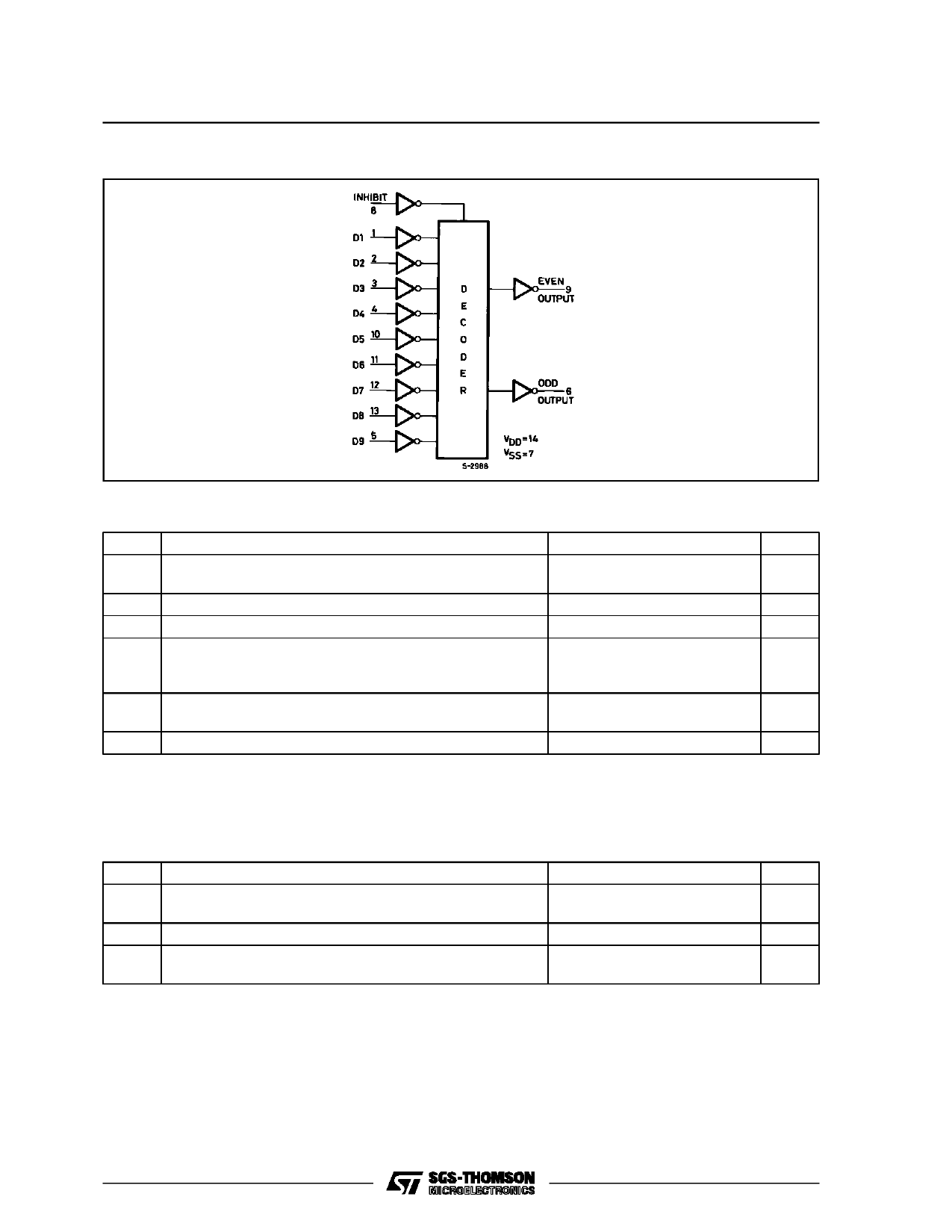
HCC/HCF40101B
FUNCTIONAL DIAGRAM
ABSOLUTE MAXIMUM RATINGS
Symbol
Parameter
Value
Unit
V DD* Supply Voltage : HC C Types
H C F Types
– 0.5 to + 20
V
– 0.5 to + 18
V
Vi Input Voltage
II
DC Input Current (any one input)
– 0.5 to VDD + 0.5
V
± 10
mA
Pt o t Total Power Dissipation (per package)
Dissipation per Output Transistor
for To p = Full Package-temperature Range
200
mW
100
mW
T o p Operating Temperature : HCC Types
H CF Types
– 55 to + 125
°C
– 40 to + 85
°C
Ts tg Storage Temperature
– 65 to + 150
°C
Stresses above those listed under ”Absolute Maximum Ratings” may cause permanent damage to the device. This is a stress
rating only and functional operation of the device at these or any other conditions above those indicated in the operational sections
of this specification is not implied. Exposure to absolute maximum rating conditions for external periods may affect device reliabili ty.
* All voltages are with respect to VSS (GND).
RECOMMENDED OPERATING CONDITIONS
Symbol
Parameter
VDD Supply Voltage : H CC Types
H C F Types
VI Input Voltage
T o p Operating Temperature : HCC Types
H CF Types
Value
3 to 18
3 to 15
0 to VDD
– 55 to + 125
– 40 to + 85
Unit
V
V
V
°C
°C
2/11
Share Link: 