HD74HC375 Ver la hoja de datos (PDF) - Renesas Electronics
Número de pieza
componentes Descripción
Lista de partido
HD74HC375 Datasheet PDF : 7 Pages
| |||
HD74HC375
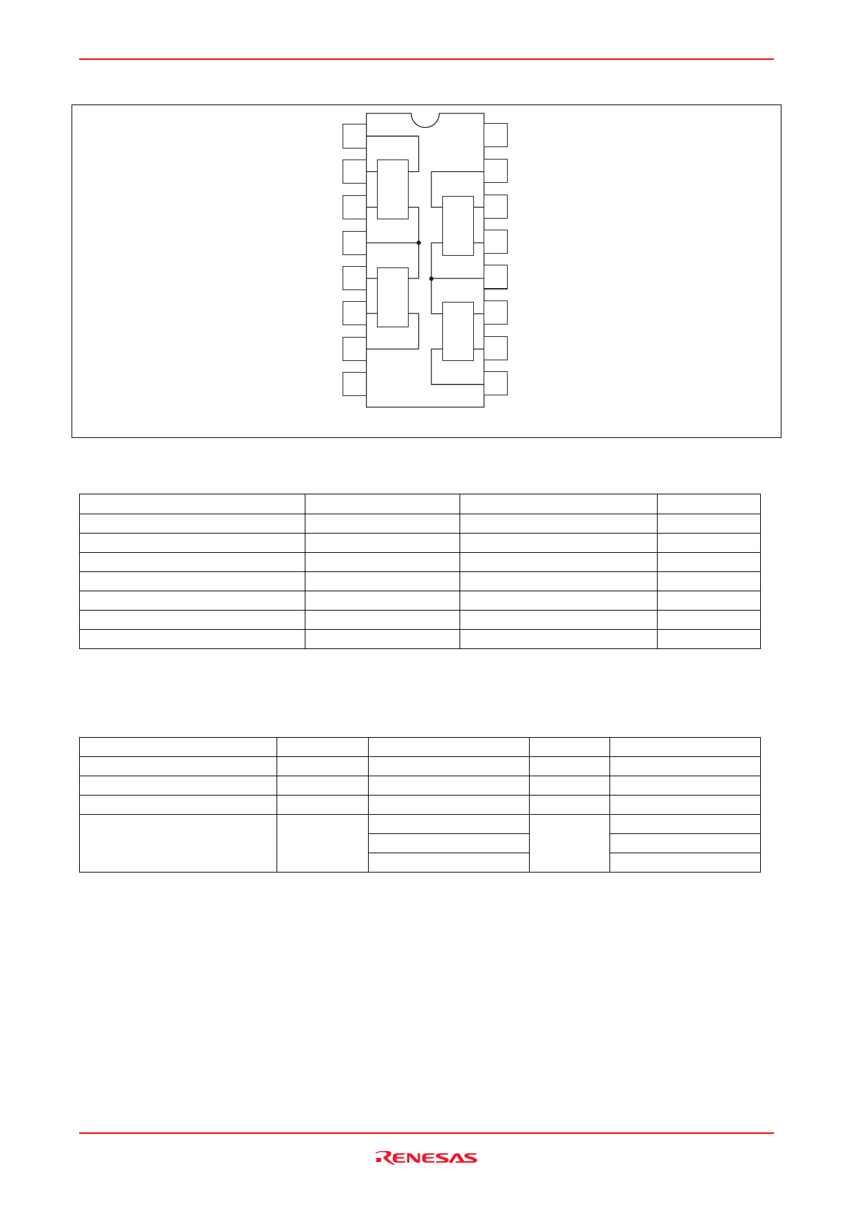
Pin Arrangement
1D 1
16 VCC
1Q 2 Q D
15 4D
1Q 3
Enable
1 to 2 4
2Q 5
QC
QC
2Q 6 Q D
D Q 14 4Q
C Q 13 4Q
12
Enable
3 to 4
C Q 11 3Q
2D 7
D Q 10 3Q
GND 8
9 3D
(Top view)
Absolute Maximum Ratings
Item
Symbol
Ratings
Unit
Supply voltage range
VCC
–0.5 to 7.0
V
Input / Output voltage
VIN, VOUT
–0.5 to VCC +0.5
V
Input / Output diode current
IIK, IOK
±20
mA
Output current
IOUT
±25
mA
VCC, GND current
ICC or IGND
±50
mA
Power dissipation
PT
500
mW
Storage temperature
Tstg
–65 to +150
°C
Note: The absolute maximum ratings are values, which must not individually be exceeded, and furthermore, no two of
which may be realized at the same time.
Recommended Operating Conditions
Item
Symbol
Ratings
Supply voltage
VCC
2 to 6
Input / Output voltage
VIN, VOUT
0 to VCC
Operating temperature
Ta
–40 to 85
Input rise / fall time*1
0 to 1000
tr, tf
0 to 500
0 to 400
Note: 1. This item guarantees maximum limit when one input switches.
Waveform: Refer to test circuit of switching characteristics.
Unit
V
V
°C
ns
Conditions
VCC = 2.0 V
VCC = 4.5 V
VCC = 6.0 V
Rev.2.00 Mar 30, 2006 page 2 of 6
Share Link: 