HIP6020A(1999) Ver la hoja de datos (PDF) - Intersil
Número de pieza
componentes Descripción
Lista de partido
HIP6020A Datasheet PDF : 16 Pages
| |||
HIP6020A
+5VIN
LIN
VOUT2
CIN
+12V
COCSET2 CVCC
VCC GND
COCSET1
ROCSET2
Q3
LOUT2
COUT2 CR2
OCSET2 OCSET1
UGATE2
UGATE1
PHASE2
PHASE1
ROCSET1
Q1
LOUT1
VOUT1
LGATE1
SS
Q2
COUT1
CR1
VOUT3
CSS
HIP6020A
VOUT4
COUT3
Q4
DRIVE3 DRIVE4
PGND
COUT4
Q5
+3.3VIN
KEY
ISLAND ON POWER PLANE LAYER
ISLAND ON CIRCUIT PLANE LAYER
VIA CONNECTION TO GROUND PLANE
FIGURE 7. PRINTED CIRCUIT BOARD POWER PLANES AND
ISLANDS
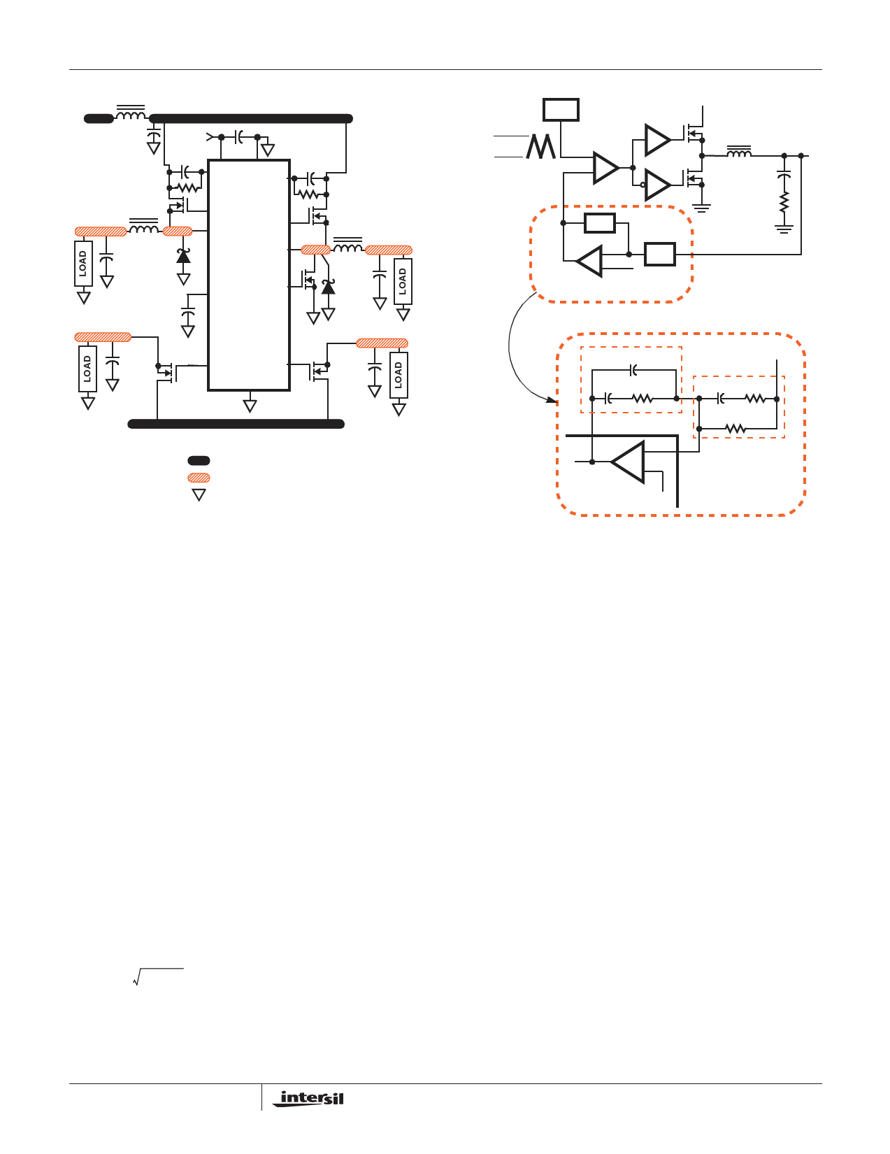
PWM1 Controller Feedback Compensation
Both PWM controllers use voltage-mode control for output
regulation. This section highlights the design consideration
for a voltage-mode controller requiring external
compensation. Apply these methods and considerations
only to the synchronous PWM controller. The considerations
for the standard PWM controller are presented separately.
Figure 11 highlights the voltage-mode control loop for a
synchronous-rectified buck converter. The output voltage
(VOUT) is regulated to the Reference voltage level. The
reference voltage level is the DAC output voltage (DACOUT) for
PWM1. The error amplifier output (VE/A) is compared with the
oscillator (OSC) triangular wave to provide a pulse-width
modulated wave with an amplitude of VIN at the PHASE node.
The PWM wave is smoothed by the output filter (LO and CO).
The modulator transfer function is the small-signal transfer
function of VOUT/VE/A. This function is dominated by a DC
Gain, given by VIN/VOSC, and shaped by the output filter, with
a double pole break frequency at FLC and a zero at FESR.
Modulator Break Frequency Equations
FLC=
-------------------1--------------------
2π × LO × CO
FESR= 2----π-----×-----E----S--1---R------×----C-----O---
The compensation network consists of the error amplifier
(internal to the HIP6020A) and the impedance networks ZIN
and ZFB. The goal of the compensation network is to provide a
4-11
∆VOSC
OSC
PWM
COMP
-
+
VIN
DRIVER
LO
VOUT
DRIVER
PHASE
CO
VE/A
ZFB
-
+
ERROR
AMP
ZIN
REFERENCE
ESR
(PARASITIC)
DETAILED COMPENSATION COMPONENTS
C2
C1 R2
ZFB
VOUT
ZIN
C3 R3
R1
COMP
FB
-
+
HIP6020A
DACOUT
FIGURE 8. VOLTAGE-MODE BUCK CONVERTER
COMPENSATION DESIGN
closed loop transfer function with high 0dB crossing frequency
(f0dB) and adequate phase margin. Phase margin is the
difference between the closed loop phase at f0dB and 180
degrees. The equations below relate the compensation
network’s poles, zeros and gain to the components (R1, R2,
R3, C1, C2, and C3) in Figure 11. Use these guidelines for
locating the poles and zeros of the compensation network:
1. Pick Gain (R2/R1) for desired converter bandwidth
2. Place 1ST Zero Below Filter’s Double Pole (~75% FLC)
3. Place 2ND Zero at Filter’s Double Pole
4. Place 1ST Pole at the ESR Zero
5. Place 2ND Pole at Half the Switching Frequency
6. Check Gain against Error Amplifier’s Open-Loop Gain
7. Estimate Phase Margin - Repeat if Necessary
Compensation Break Frequency Equations
FZ1 = 2----π-----×-----R---1--2-----×----C-----1--
FP1
=
---------------------------1---------------------------
2π
×
R2
×
C-C----11-----+×-----CC-----22--
FZ2 = 2----π-----×-----(--R-----1-----+-1----R-----3---)----×-----C-----3-
FP2 = -2---π-----×-----R---1--3-----×----C-----3--
Figure 12 shows an asymptotic plot of the DC-DC converter’s
gain vs. frequency. The actual Modulator Gain has a high gain
peak dependent on the quality factor (Q) of the output filter,
which is not shown in Figure 12. Using the above guidelines
should yield a Compensation Gain similar to the curve plotted.
The open loop error amplifier gain bounds the compensation
Share Link: 