HSP50214AVC Ver la hoja de datos (PDF) - Intersil
Número de pieza
componentes Descripción
Lista de partido
HSP50214AVC Datasheet PDF : 60 Pages
| |||
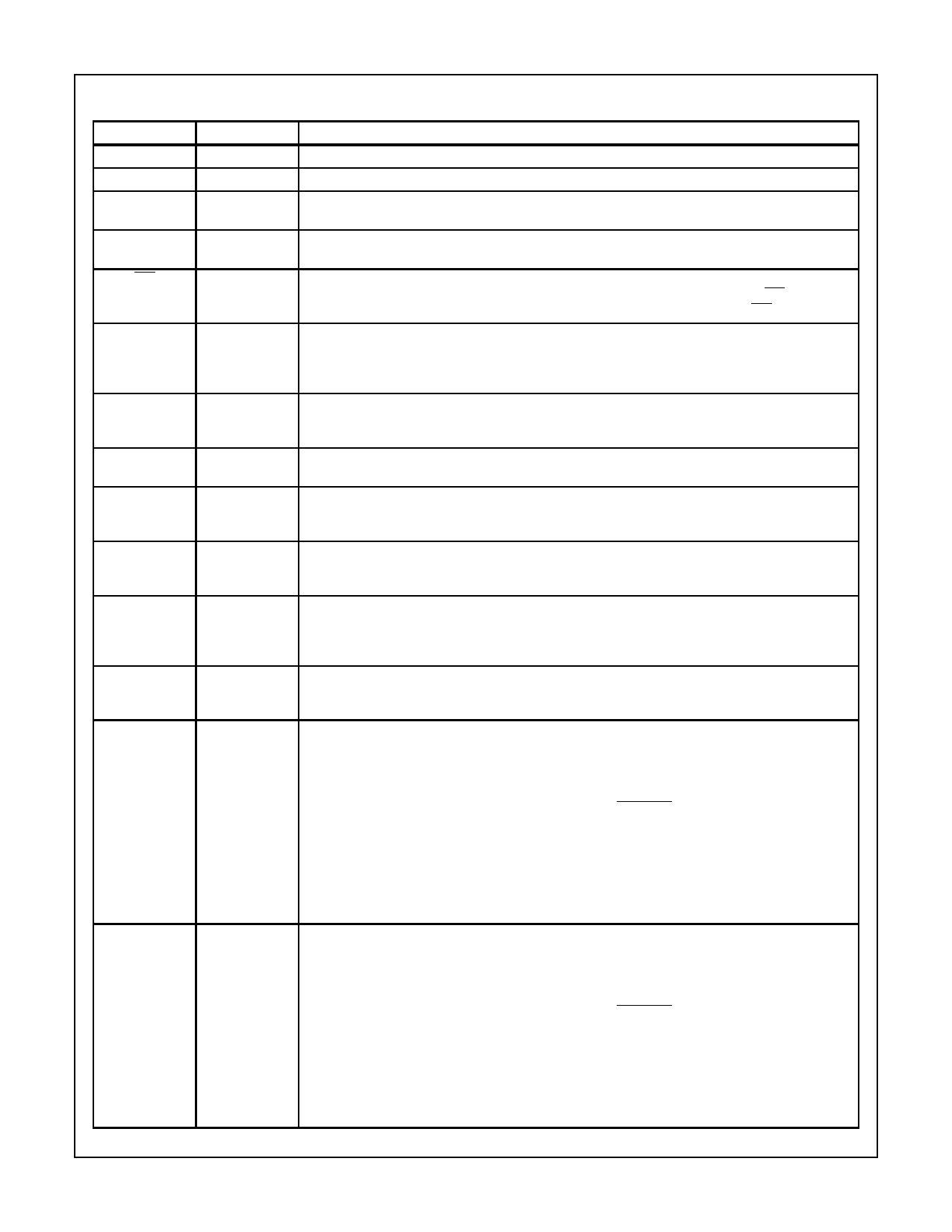
Pin Descriptions
NAME
VCC
GND
CLKIN
TYPE
-
-
I
IN(13:0)
I
ENI
I
GAINADJ(2:0)
I
PROCCLK
I
AGCGNSEL
I
COF
I
COFSYNC
I
SOF
I
SOFSYNC
I
AOUT(15:0)
O
BOUT(15:0)
O
HSP50214A
DESCRIPTION
Positive Power Supply Voltage.
Ground.
Input Clock. This clock should be a multiple of the input sample rate. All input section processing oc-
curs on the rising edge of CLKIN. The frequency of CLKIN is designated fCLKIN.
Input Data. The format of the input data may be set to offset binary or 2’s complement. IN13 is the
MSB (see Control Word 0).
Input Enable. Active Low. This pin enables the input to the part in one of two modes, gated or inter-
polated (see Control Word 0). In gated mode, one sample is taken per CLKIN when ENI is asserted.
The input sample rate is designated fS, which can be different from fCLKIN When ENI is used.
GAINADJ Input. Adds an offset to the gain via the shifter following the mixer. GAINADJ value is added
to the shift code from the microprocessor (µP) interface. The shift code is saturated to a maximum
code of F. The gain is offset by (6dB)(GAINADJ); (000 = 0dB gain adjust; 111 = 42dB gain adjust)
GAINADJ2 is the MSB. See “Using the Input Gain Adjust Control Signals” Section.
Processing Clock. PROCCLK is the clock for all processing functions following the CIC Section. Pro-
cessing is performed on PROCCLK’s rising edge. All output timing is derived from this clock.
NOTE: This clock may be asynchronous to CLKIN.
AGC Gain Select. This pin selects between two AGC loop gains. This input is setup and held relative
to PROCCLK. Gain setting 1 is selected when AGCGNSEL = 1.
Carrier Offset Frequency Input. This serial input pin is used to load the carrier offset frequency into the
Carrier NCO (see Serial Interface Section). The offset may be 8, 16, 24, or 32 bits. The setup and hold
times are relative to CLKIN. This input is compatible with the output of the HSP50210 Costas loop [1].
Carrier Offset Frequency Sync. This signal is asserted one CLK before the most significant bit (MSB)
of the offset frequency word (see Serial Interface Section). The setup and hold times are relative to
CLKIN. This input is compatible with the output of the HSP50210 Costas loop [1].
Re-Sampler Offset Frequency Input. This serial input pin is used to load the offset frequency into the
Re-Sampler NCO (see Serial Interface Section). The offset may be 8, 16, 24, or 32 bits. The setup
and hold times are relative to PROCCLK. This input is compatible with the output of the HSP50210
Costas loop [1].
Re-Sampler Offset Frequency Sync. This signal is asserted one CLK before the MSB of the offset
frequency word (see Serial Interface Section). The setup and hold times are relative to PROCCLK.
This input is compatible with the output of the HSP50210 Costas loop [1].
Parallel Output Bus A. Two parallel output modes are available on the HSP50214A. The first is called
the Direct Output Port, where the source is selected through Control Word 20 (see the Microproces-
sor Write Section) and comes directly from the Output MUX Section (see Output Control Section).
The most significant byte of AOUT always outputs the most significant byte of the Parallel Direct Out-
put Port whose data type is selected via µP interface. AOUT15 is the MSB. In this mode, the
AOUT(15:0) bus is updated as soon as data is available. DATARDY is asserted to indicate new data.
The second mode for parallel data is called the Buffer RAM Output Port. The Buffer RAM Output Port
acts like a FIFO for blocks of information called data sets. Within a data set is I, Q, magnitude, phase,
and frequency information; a data type is selected using SEL(2:0). Up to 7 data sets are stored in the
Buffer RAM Output Port. The LSBytes of the AOUT and BOUT busses form the 16 bits for the buffered
output mode and can be used for buffered mode while the MSBytes are outputting data in the direct
output mode.
Parallel Output Bus B. Two parallel output modes are available on the HSP50214A. The first is called
the Direct Output Port, where the source is selected through Control Word 20 (see the Microproces-
sor Write Section) and comes directly from the Output MUX Section (see Output Control Section).
The most significant byte of BOUT always outputs the most significant byte of the Parallel Direct Out-
put Port whose data type is selected via µP interface. BOUT15 is the MSB. In this mode, the
BOUT(15:0) bus is updated as soon as data is available. DATARDY is asserted to indicate new data.
The second mode for parallel data is called the Buffer RAM Output Port. The Buffer RAM Output Port
acts like a FIFO for blocks of information called data sets. Within a data set is I, Q, magnitude, phase,
and frequency information; a particular information is selected using SEL(2:0). Up to 7 data sets is
stored in the Buffer RAM Output Port. The least significant byte of BOUT can be used to either output
the least significant byte of the B Parallel Direct Output Port or the least significant byte of the Buffer
RAM Output Port. See Output Section.
3
Share Link: 