HT1650(2005) Ver la hoja de datos (PDF) - Holtek Semiconductor
Número de pieza
componentes Descripción
Lista de partido
HT1650 Datasheet PDF : 18 Pages
| |||
HT1650
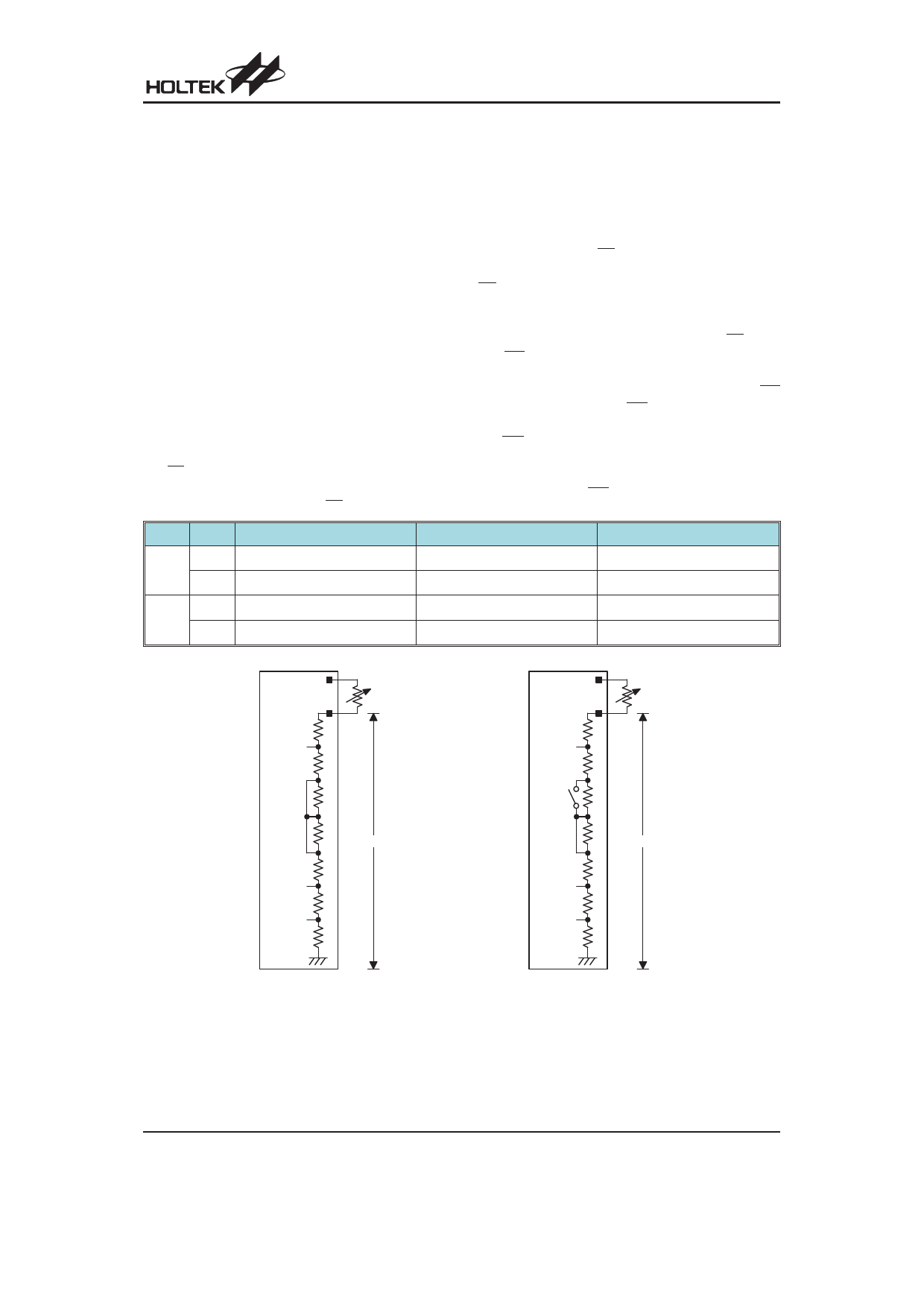
Bias Generator
The HT1650 bias voltage belongs to the internal resistor
type. It provides two kinds of bias options, namely 1/6
bias and 1/5 bias respectively. It also provides three
kinds of bias current options by programming to suitably
drive an LCD panel. The three kinds of bias current are
large, middle, and small, respectively. Usually, large
panel LCD can be excellently displayed by large bias
current. Relatively, it consumes large current when LCD
ON command is used. Small bias current provides low
power consumption during on condition when the LCD
is normally displayed. The following are the reference
value table.
When the bias current for LCD is more than Large Bias
Current setting. It is recommended to add external cir-
cuit to increase driving current.
Interfacing
Only six lines are required to interface with the HT1650.
The CS line is used to initialize the serial interface circuit
and to terminate the communication between the host
controller and the HT1650. If the CS pin is set to 1, the
data and command issued between the host controller
and the HT1650 are first disabled and then initialized.
Before issuing a mode command or mode switching, a
high level pulse is required to initialize the serial inter-
face of the HT1650. The DB0~DB3 are the 4-bit parallel
data input/output lines. Data to be read or written or
commands to be written have to pass through the
DB0~DB3 lines. The RD line is the READ clock input.
Data in the RAM are clocked out on the falling edge of the
RD signal, and the clocked out data will then appear on
the DB0~DB3 lines. It is recommended that the host
controller read correct data during the interval between
the rising edge and the next falling edge of the RD signal.
The WR line is the WRITE clock input. The data, ad-
dress, and command on the DB0~DB3 lines are all
clocked into the HT1650 on the rising edge of the WR
signal. There is an optional IRQ line to be used as an in-
terface between the host controller and the HT1650.
The IRQ pin can be selected as a timer output or a WDT
overflow flag output by the S/W setting. The host con-
troller can perform the time base or the WDT function by
connecting with the IRQ pin of the HT1650.
Bias VLCD
Large Bias Current
Middle Bias Current
Small Bias Current
3V
1/5
5V
165mA
270mA
70mA
110mA
30mA
50mA
3V
1/6
5V
140mA
225mA
55mA
90mA
25mA
40mA
P ow er
P ow er
V LC D
VR
R
(T 1 ) V 1
R
(T 2 ) V 2
R
V3
R
V LC D
V4
R
(T 3 ) V 5
R
(T 4 ) V 6
R
VSS
1 /5 B ia s
V LC D
VR
R
(T 1 ) V 1
R
(T 2 ) V 2
R
V3
R
V LC D
V4
R
(T 3 ) V 5
R
(T 4 ) V 6
R
VSS
1 /6 B ia s
Internal Resistor Type Bias Generator Configurations
Note: The voltage applied to VLCD pin must be lower than 7V
Adjust VR to fit LCD display
Rev. 1.20
11
November 10, 2005
Share Link: 