HT1670 Ver la hoja de datos (PDF) - Holtek Semiconductor
Número de pieza
componentes Descripción
Lista de partido
HT1670 Datasheet PDF : 20 Pages
| |||
PATENTED
HT1670
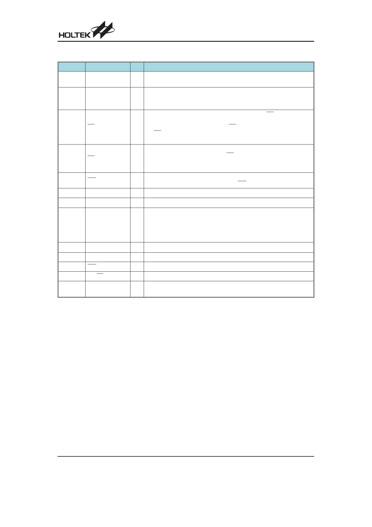
Pad Description
Pad No.
Pad Name
1~42
96~181
SEG86~SEG127
SEG0~SEG85
43~58
80~95
COM31~COM16
COM0~COM15
59
CS
60
RD
61
62~65
66
WR
DB0~DB3
VSS
67
OSCI
68
OSCO
69
70, 79
71
72, 73
74~78
VDD
VLCD
IRQ
BZ, BZ
T1~T4, T000
I/O
Description
O LCD segment outputs
LCD common outputs, under 144´16 command mode, COM16~COM31 will
O share to SEG128~SEG143. COM31/SEG128, COM30/SEG129, COM29/
SEG130....., COM18/SEG141, COM17/SEG142, COM16/SEG143
Chip selection input with pull-high resistor. When the CS is logic high, the
data and command read from or write to the HT1670 are disabled. The serial
I interface circuit is also reset. But if the CS is at a logic low level and is input to
the CS pad, the data and command transmission between the host controller
and the HT1670 are all enabled.
READ clock input with pull-high resistor. Data in the RAM of the HT1670 are
I
clocked out on the falling edge of the RD signal. The clocked out data will ap-
pear on the data line. The host controller can use the next rising edge to latch
the clocked out data.
I
WRITE clock input with pull-high resistor. Data on the DATA line are latched
into the HT1670 on the rising edge of the WR signal.
I/O Parallel data input/output with a pull-high resistor
¾ Negative power supply for logic circuit, ground
The OSCI and OSCO pads are connected to a 32.768kHz crystal in order to
I
O
generate a system clock. If the system clock comes from an external clock
source, the external clock source should be connected to the OSCI pad. But
if an on-chip RC oscillator is selected, the OSCI and OSCO pads can be left
open.
¾ Positive power supply for logic circuit
I Power supply for LCD driver circuit
O Time base or Watchdog Timer overflow flag, NMOS open drain output.
O 2kHz or 4kHz frequency output pair (tristate output buffer)
I
Vary bias current pin
It is usually not connected
Absolute Maximum Ratings
Supply Voltage ...........................VSS-0.3V to VSS+5.5V
Input Voltage.............................VSS-0.3V to VDD+0.3V
Storage Temperature ............................-50°C to 125°C
Operating Temperature...........................-25°C to 75°C
Note: These are stress ratings only. Stresses exceeding the range specified under ²Absolute Maximum Ratings² may
cause substantial damage to the device. Functional operation of this device at other conditions beyond those listed
in the specification is not implied and prolonged exposure to extreme conditions may affect device reliability.
Rev. 1.60
5
November 9, 2010
Share Link: 