HY57V161610D Ver la hoja de datos (PDF) - Hynix Semiconductor
Número de pieza
componentes Descripción
Lista de partido
HY57V161610D Datasheet PDF : 13 Pages
| |||
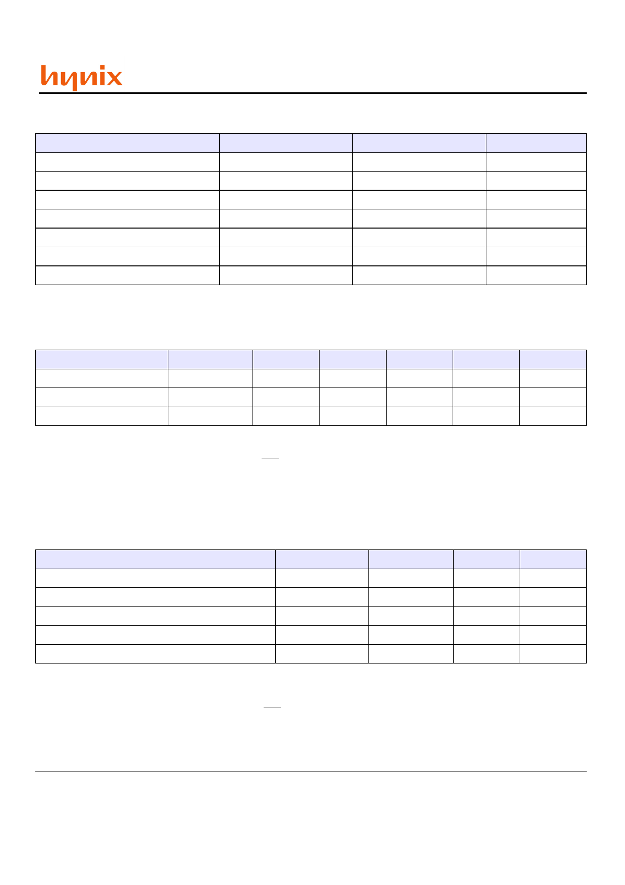
ABSOLUTE MAXIMUM RATINGS
Parameter
Ambient Temperature
Storage Temperature
Voltage on Any Pin relative to VSS
Voltage on VDD relative to VSS
Short Circuit Output Current
Power Dissipation
Soldering Temperature·Time
Symbol
TA
TSTG
VIN, VOUT
VDD
IOS
PD
TSOLDER
Rating
0 ~ 70
-55 ~ 125
-1.0 ~ 4.6
-1.0 ~ 4.6
50
1
260·10
Note : Operation at above absolute maximum rating can adversely affect device reliability.
DC OPERATING CONDITION (TA=0°C to 70°C)
Parameter
Power Supply Voltage
Input high voltage
Input low voltage
Symbol
VDD, VDDQ
VIH
VIL
Min
Typ.
3.0
3.3
2.0
3.0
-0.5
0
Note :
1.All voltages are referenced to VSS = 0V.
2.VDD(min) is 3.15V when HY57V161610DTC-7 operates at CAS latency=2
3.VDD(min) of HY57V161610DTC-5/55 is 3.15V
4.VIH(max) is acceptable 4.6V AC pulse width with ≤ 10ns of duration.
5.VIL(min) is acceptable -1.5V AC pulse width with ≤ 10ns of duration.
Max
3.6
VDD + 0.3
0.8
AC OPERATING CONDITION (TA=0°C to 70°C, VDD=3.0V to 3.6V, VSS=0V)
Parameter
AC input high / low level voltage
Input timing measurement reference level voltage
Input rise / fall time
Output timing measurement reference level
Output load capacitance for access time measurement
Symbol
VIH / VIL
Vtrip
tR / tF
Voutref
CL
Value
2.4/0.4
1.4
1
1.4
30
Note :
1. Output load to measure access times is equivalent to two TTL gates and one capacitance(30pF).
For details, refer to AC/DC output load circuit.
2. VDD(min) is 3.15V when HY57V161610DTC-7 operates at CAS latency=2 and tCK2=8.9ns
3. VDD(min) of HY57V161610DTC-5/55 is 3.15V‘
HY57V161610D
Unit
°C
°C
V
V
mA
W
°C ·Sec
Unit
Note
V
1, 2, 3
V
1, 4
V
1, 5
Unit
Note
V
V
ns
V
pF
1
Rev. 4.0/Aug. 02
4
Share Link: 