ICL7665 Ver la hoja de datos (PDF) - Intersil
Número de pieza
componentes Descripción
Lista de partido
ICL7665 Datasheet PDF : 11 Pages
| |||
ICL7665S
Absolute Maximum Ratings
Supply Voltage (Note 2) . . . . . . . . . . . . . . . . . . . . . . . . . -0.3 to +18V
Output Voltages OUT1 and OUT2 . . . . . . . . . . . . . . . . . -0.3V to 18V
(with respect to GND) (Note 2)
Output Voltages HYST1 and HYST2 . . . . . . . . . . . . . . -0.3V to +18V
(with respect to V+) (Note 2)
Input Voltages SET1 and SET2 . . . . . (GND -0.3V) to (V+ V- +0.3V)
(Note 2)
Maximum Sink Output OUT1 and OUT2 . . . . . . . . . . . . . . . . . 25mA
Maximum Source Output Current
HYST1 and HYST2 . . . . . . . . . . . . . . . . . . . . . . . . . . . . . . -25mA
Thermal Information
Thermal Resistance (Typical, Note 1)
θJA (oC/W) θJC (oC/W)
PDIP Package . . . . . . . . . . . . . . . . . . . 150
N/A
Plastic SOIC Package . . . . . . . . . . . . . 180
N/A
Maximum Junction Temperature (Plastic) . . . . . . . . . . . . . . . .150oC
Maximum Junction Temperature (CERDIP). . . . . . . . . . . . . . .175oC
Maximum Storage Temperature Range . . . . . . . . . . -65oC to 150oC
Maximum Lead Temperature (Soldering 10s) . . . . . . . . . . . . .300oC
(SOIC - Lead Tips Only)
Operating Conditions
Temperature Range
ICL7665SC. . . . . . . . . . . . . . . . . . . . . . . . . . . . . . . . . 0oC to 70oC
ICL7665SI . . . . . . . . . . . . . . . . . . . . . . . . . . . . . . . -40oC to 85oC
CAUTION: Stresses above those listed in “Absolute Maximum Ratings” may cause permanent damage to the device. This is a stress only rating and operation of the
device at these or any other conditions above those indicated in the operational sections of this specification is not implied.
NOTES:
1. θJA is measured with the component mounted on an evaluation PC board in free air.
2. Due to the SCR structure inherent in the CMOS process used to fabricate these devices, connecting any terminal to voltages greater than (V+
+0.3V) or less than (GND - 0.3V) may cause destructive device latchup. For these reasons, it is recommended that no inputs from external
sources not operating from the same power supply be applied to the device before its supply is established, and that in multiple supply systems,
the supply to the ICL7665S be turned on first. If this is not possible, current into inputs and/or outputs must be limited to ±0.5mA and voltages
must not exceed those defined above.
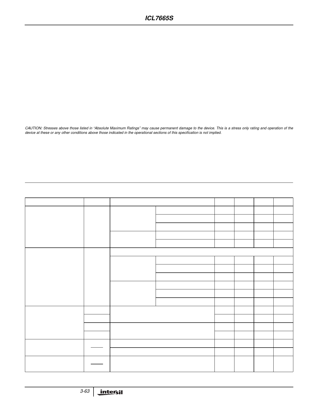
Electrical Specifications The specifications below are applicable to both the ICL7665S and ICL7665SA. V+ = 5V, TA = 25oC,
Test Circuit Figure 7. Unless Otherwise Specified
PARAMETER
Operating Supply Voltage
Supply Current
SYMBOL
TEST CONDITIONS
MIN
TYP
MAX UNITS
V+
ICL7665S
ICL7665SA
TA = 25oC
0oC ≤ TA ≤ 70oC
-25oC ≤ TA ≤ 85oC
0oC ≤ TA ≤ 70oC
-25oC ≤ TA ≤ 85oC
1.6
-
16
V
1.8
-
16
V
1.8
-
16
V
1.8
-
16
V
1.8
-
16
V
I+
GND ≤ VSET1, VSET2 ≤ V+, All Outputs Open Circuit
0oC ≤ TA ≤ 70oC
V+ = 2V
-
2.5
10
µA
V+ = 9V
-
2.6
10
µA
-40oC ≤ TA ≤ 85oC
V+ = 15V
V+ = 2V
V+ = 9V
-
2.9
10
µA
-
2.5
10
µA
-
2.6
10
µA
V+ = 15V
-
2.9
10
µA
Input Trip Voltage
Temperature Coefficient of
VSET
VSET1
VSET2
VSET1
VSET2
∆VSET
∆T
ICL7665S
ICL7665SA
ICL7665S
ICL7665SA
1.20
1.30
1.40
V
1.20
1.30
1.40
V
1.275 1.30 1.325
V
1.275 1.30 1.325
V
-
200
-
ppm
-
100
-
ppm
Supply Voltage Sensitivity of
VSET1, VSET2
∆VSET
∆VS
ROUT1, ROUT2, RHYST1, R2HYST2 = 1MΩ,
2V ≤ V+ ≤ 10V
-
0.03
-
%/V
3-63
Share Link: 