ICS650-41 Ver la hoja de datos (PDF) - Integrated Circuit Systems
Número de pieza
componentes Descripción
Lista de partido
ICS650-41 Datasheet PDF : 11 Pages
| |||
ICS650-41
Spread Spectrum Clock Synthesizer
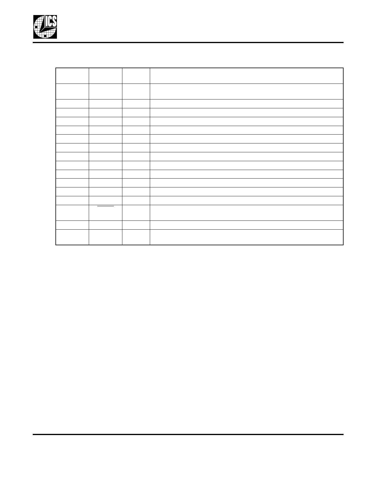
Pin Descriptions
Pin
Number
1
2
3
4
5
6
7
8
9
10
11
12
13
14
15
16
Pin Name
X1/CLKIN
FS0
FS1
SS_EN
VDD
GND
FS3
48M
50M
VDDO
GND
VDD
FS2
PDTS
VDD
X2
Pin
Type
Input
Input
Input
Input
Power
Power
Input
Output
Output
Power
Power
Power
Input
Input
Power
Output
Pin Description
Crystal input. Connect this pin to a 25 MHz crystal or external input
clock.
Select pin 0. Internal pull-up resistor. See table on page 2.
Select pin 1. Internal pull-up resistor. See table on page 2.
Spread spectrum enable pin. Internal pull-up resistor. Enabled = high.
Connect to +3.3 V.
Connect to ground.
Select pin 3. Internal pull-up resistor. See table on page 2.
Fixed 48 MHz output. Weak internal pull-down when tri-state.
Spread Spectrum output. Weak internal pull-down when tri-stated.
Connect to +2.5 V.
Connect to ground.
Connect to +3.3 V.
Select pin 2. Internal pull-up resistor. See table on page 2.
Powers down entire chip. Tri-states CLK outputs when low. Internal
pull-up.
Connect to +3.3 V.
Crystal Output. Connect this pin to a 25 MHz crystal. Do not connect if
clock input is used.
External Components
Decoupling Capacitor
As with any high-performance mixed-signal IC, the
ICS650-41 must be isolated from system power supply
noise to perform optimally.
A decoupling capacitor of 0.01µF must be connected
between each VDD and the PCB ground plane.
Series Termination Resistor
Clock output traces over one inch should use series
termination. To series terminate a 50Ω trace (a
commonly used trace impedance), place a 33Ω resistor
in series with the clock line, as close to the clock output
pin as possible. The nominal impedance of the clock
output is 20Ω.
Crystal Load Capacitors
The device crystal connections should include pads for
small capacitors from X1 to ground and from X2 to
ground. These capacitors are used to adjust the stray
capacitance of the board to match the nominally
required crystal load capacitance. Because load
capacitance can only be increased in this trimming
process, it is important to keep stray capacitance to a
minimum by using very short PCB traces (and no vias)
between the crystal and device. Crystal capacitors
must be connected from each of the pins X1 and X2 to
ground.
The value (in pF) of these crystal caps should equal
(CL -6 pF)*2. In this equation, CL= crystal load
capacitance in pF. Example: For a crystal with a 16 pF
load capacitance, each crystal capacitor would be 20
pF [(16-6) x 2] = 20.
MDS 650-41 F
3
Revision 082305
Integrated Circuit Systems, Inc. ● 525 Race Street, San Jose, CA 95126 ● tel (408) 297-1201 ● www.icst.com
Share Link: 