ICSSSTU32864 Ver la hoja de datos (PDF) - Integrated Circuit Systems
Número de pieza
componentes Descripción
Lista de partido
ICSSSTU32864 Datasheet PDF : 11 Pages
| |||
ICSSSTU32864
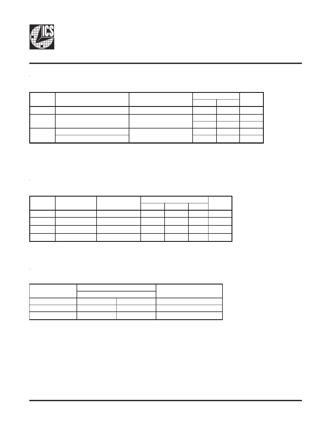
Timing Requirements
(over recommended operating free-air temperature range, unless otherwise noted)
SYMBOL
PARAMETERS
VDD = 1.8V ±0.1V
MIN MAX
fclock Clock frequency
300
tS Setup time
Data before CLK↑, CLK#↓
0.75
0.9
Th
Hold time, fast slew rate 2, 4
Hold time, slow slew rate 3, 4
Data after CLK↑, CLK#↓
0.50
0.70
Notes: 1 - Guaranteed by design, not 100% tested in production.
2 - For data signal input slew rate of 1V/ns.
3 - For data signal input slew rate of 0.5V/ns and < 1V/ns.
4 - CLK/CLK# signal input slew rate of 1V/ns.
UNITS
MHz
ns
ns
ns
ns
Switching Characteristics
(over recommended operating free-air temperature range, unless otherwise noted)
SYMBOL
From
(Input)
To
(Output)
VDD = 1.8V ±0.1V
MIN
TYP MAX
UNITS
fmax
tPDM1
tPDMSS2
CLK, CLK#
CLK, CLK#
270
Q
1.41
Q
MHz
1.85
ns
tphl RESET#
Q
3
ns
Notes: 1. Includes 350ps test-load transmission-line delay
2. Guaranteed by design, not 100% tested in production.
Output Buffer Characteristics
Output edge rates over recommended operating free-air temperature range (See figure 7)
PARAMETER
VDD = 1.8V ± 0.1V
MIN
MAX
UNIT
dV/dt_r
1
4
V/ns
dV/dt_f
1
4
dV/dt_∆ 1
1
V/ns
V/ns
1. Difference between dV/dt_r (rising edge rate) and dV/dt_f (falling edge rate)
0727C—04/15/04
8
Share Link: 