IDT7025 Ver la hoja de datos (PDF) - Integrated Device Technology
Número de pieza
componentes Descripción
Lista de partido
IDT7025 Datasheet PDF : 20 Pages
| |||
IDT7025S/L
HIGH-SPEED 8K x 16 DUAL-PORT STATIC RAM
MILITARY AND COMMERCIAL TEMPERATURE RANGES
AC TEST CONDITIONS
Input Pulse Levels
Input Rise/Fall Times
Input Timing Reference Levels
Output Reference Levels
Output Load
GND to 3.0V
5ns Max.
1.5V
1.5V
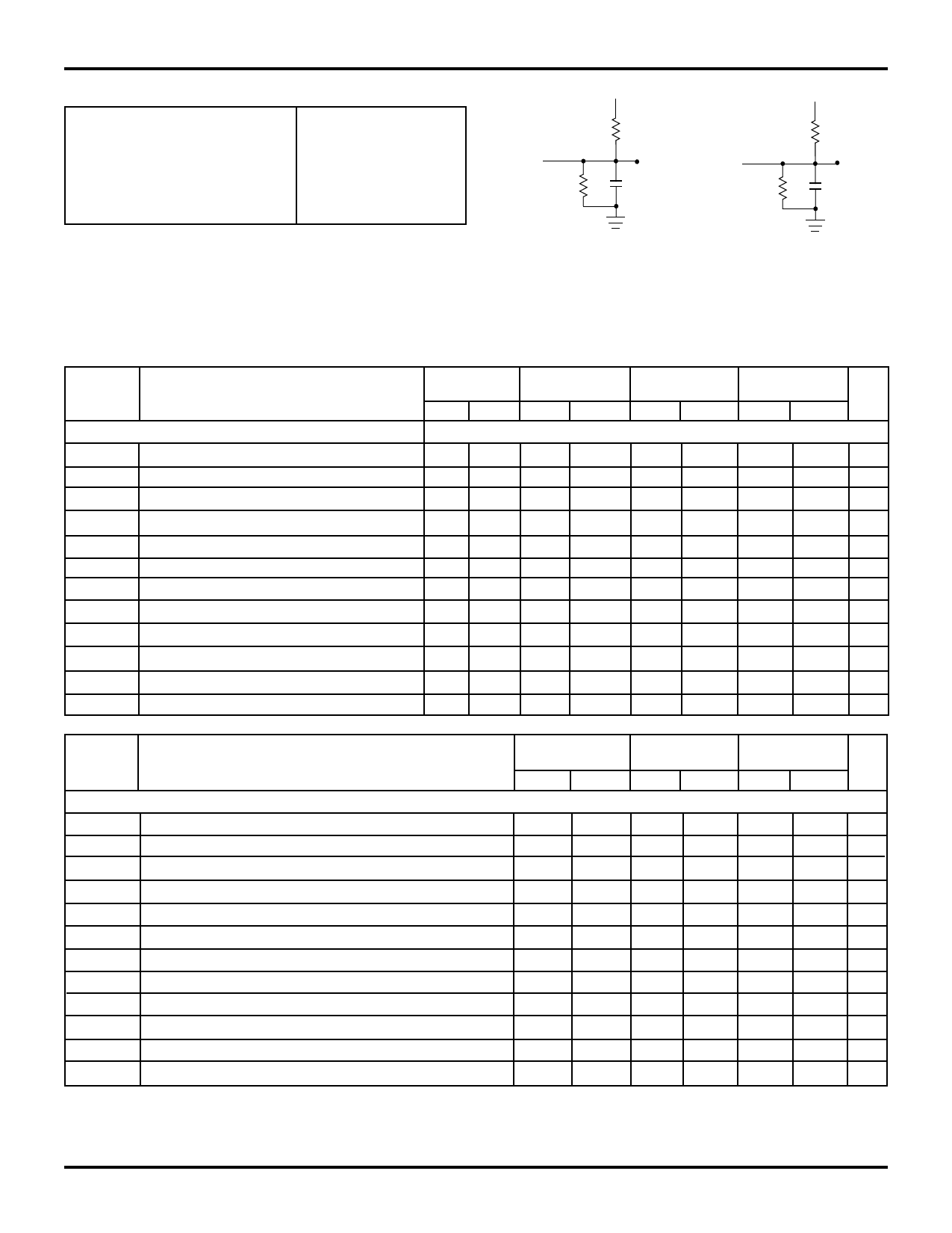
Figures 1 and 2
2683 tbl 12
DATAOUT
BUSY
INT
775Ω
5V
1250Ω
30pF
DATAOUT
775Ω
5V
1250Ω
5pF
2683 drw 06
Figure 1. AC Output Test Load
Figure 2. Output Test Load
( for tLZ, tHZ, tWZ, tOW)
* including scope and jig.
AC ELECTRICAL CHARACTERISTICS OVER THE
OPERATING TEMPERATURE AND SUPPLY VOLTAGE RANGE(4)
Symbol
Parameter
IDT7025X15
Com'l. Only
Min. Max.
IDT7025X17
Com'l. Only
Min. Max.
READ CYCLE
tRC
Read Cycle Time
15 —
17
—
tAA
Address Access Time
tACE
Chip Enable Access Time(3)
tABE
Byte Enable Access Time(3)
— 15
—
17
— 15
—
17
— 15
—
17
tAOE
Output Enable Access Time
— 10
—
10
tOH
Output Hold from Address Change
3
—
3
—
tLZ
Output Low-Z Time(1, 2)
3
—
3
—
tHZ
Output High-Z Time(1, 2)
— 10
—
10
tPU
Chip Enable to Power Up Time(1,2)
0
—
0
—
tPD
Chip Disable to Power Down Time(1,2)
— 15
—
17
tSOP
tSAA
Semaphore Flag Update Pulse (OE or SEM) 10
—
10
—
Semaphore Address Access(3)
— 15
—
17
IDT7025X20
Min. Max.
20
—
—
20
—
20
—
20
—
12
3
—
3
—
—
12
0
—
—
20
10
—
—
20
IDT7025X25
Min. Max. Unit
25
— ns
—
25 ns
—
25 ns
—
25 ns
—
13 ns
3
— ns
3
— ns
—
15 ns
0
— ns
—
25 ns
10
— ns
—
25 ns
Symbol
Parameter
READ CYCLE
tRC
Read Cycle Time
tAA
Address Access Time
tACE
Chip Enable Access Time(3)
tABE
Byte Enable Access Time(3)
tAOE
Output Enable Access Time
tOH
Output Hold from Address Change
tLZ
Output Low-Z Time(1, 2)
tHZ
Output High-Z Time(1, 2)
tPU
Chip Enable to Power Up Time(1,2)
tPD
Chip Disable to Power Down Time(1,2)
tSOP
tSAA
Semaphore Flag Update Pulse (OE or SEM)
Semaphore Address Access Time(3)
IDT7025X35
Min. Max.
IDT7025X55
Min. Max.
IDT7025X70
Mil. Only
Min. Max. Unit
35
—
55
—
70
— ns
—
35
—
55
—
70 ns
—
35
—
55
—
70 ns
—
35
—
55
—
70 ns
—
20
—
30
—
35 ns
3
—
3
—
3
— ns
3
—
3
—
3
— ns
—
15
—
25
—
30 ns
0
—
0
—
0
— ns
—
35
—
50
—
50 ns
15
—
15
—
15
— ns
—
35
—
55
—
70 ns
NOTES:
1. Transition is measured ±500mV from Low or High-impedance voltage with Output Test Load (Figure 2).
2. This parameter is guaranteed by device characterization, but is not production tested.
3. To access RAM, CE = VIL, UB or LB = VIL, and SEM = VIH. To access semephore, CE = VIH or UB & LB = VIH, and SEM = VIL.
4. "X" in part numbers indicates power rating (S or L).
2683 tbl 13
6.16
7
Share Link: 