IDT7028L(2009) Ver la hoja de datos (PDF) - Integrated Device Technology
Número de pieza
componentes Descripción
Lista de partido
IDT7028L Datasheet PDF : 17 Pages
| |||
IDT7028L
High-Speed 64K x 16 Dual-Port Static RAM
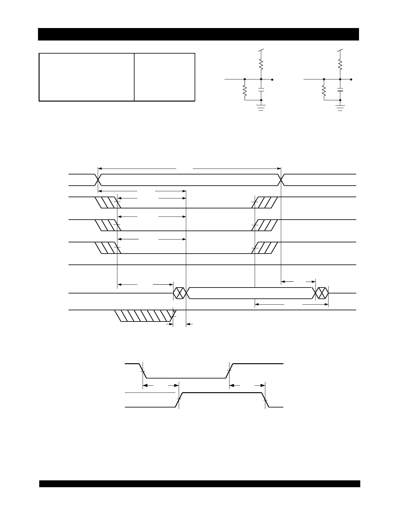
AC Test Conditions
Input Pulse Levels
Input Rise/Fall Times
Input Timing Reference Levels
Output Reference Levels
Output Load
GND to 3.0V
3ns Max.
1.5V
1.5V
Figures 1 and 2
4836 tbl 11
Industrial and Commercial Temperature Ranges
5V
5V
DATAOUT
BUSY
INT
347Ω
893Ω
DATAOUT
30pF
347Ω
893Ω
5pF*
4836 drw 03
4836 drw 04 .
Figure 1. AC Output Test Load
Figure 2. Output Test Load
(for tLZ, tHZ, tWZ, tOW)
* Including scope and jig.
Waveform of Read Cycles(5)
tRC
ADDR
CE(6)
tAA (4)
tACE (4)
tAOE (4)
OE
UB, LB
tABE (4)
R/W
DATAOUT
BUSYOUT
tLZ (1)
(4)
VALID DATA
tBDD (3,4)
tOH
tHZ (2)
4836 drw 05
Timing of Power-Up Power-Down
CE(6)
tPU
ICC
50%
tPD
50%
ISB
4836 drw 06 .
NOTES:
1. Timing depends on which signal is asserted last, OE, CE, LB or UB.
2. Timing depends on which signal is de-asserted first CE, OE, LB or UB.
3. tBDD delay is required only in cases where the opposite port is completing a write operation to the same address location. For simultaneous read operations BUSY
has no relation to valid output data.
4. Start of valid data depends on which timing becomes effective last tAOE, tACE, tAA or tBDD.
5. SEM = VIH.
6. Refer to Chip Enable Truth Table.
6
Share Link: 