IDT72205LB10TF(2000) Ver la hoja de datos (PDF) - Integrated Device Technology
Número de pieza
componentes Descripción
Lista de partido
IDT72205LB10TF
(Rev.:2000)
(Rev.:2000)
Integrated Device Technology

IDT72205LB10TF Datasheet PDF : 16 Pages
| |||
IDT72205LB/72215LB/72225LB/72235LB/72245LB CMOS SyncFIFO™
256 x 18, 512 x 18, 1,024 x 18, 2,048 x 18 and 4,096 x 18
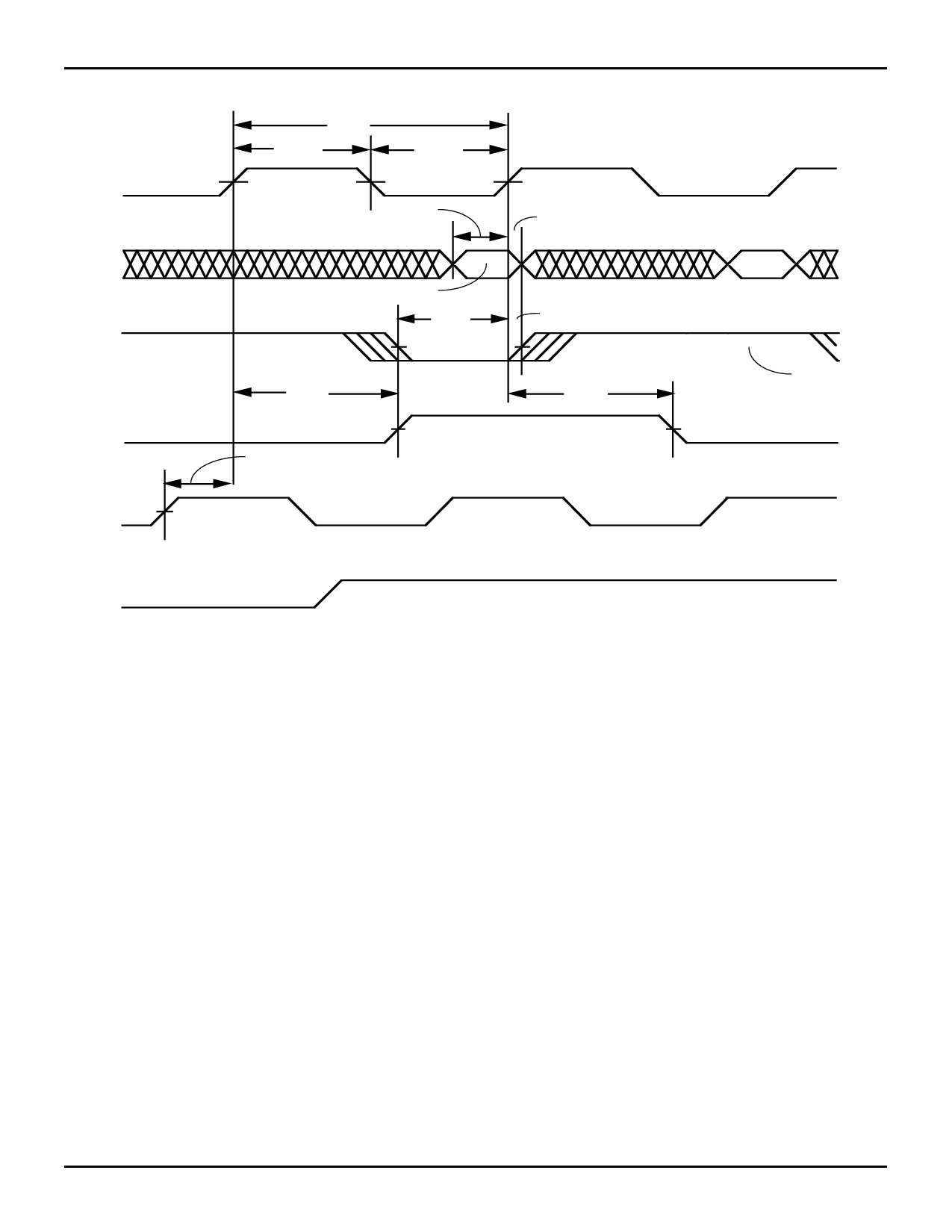
WCLK
t DS
D0 - D17
t ENS
D0 (first valid write)
D1
RCLK
tSKEW2
tFRL(1)
t REF
tENS
Commercial And Industrial Temperature Ranges
D2
D3
D4
Q0 - Q17
t OLZ
tA
t OE
tA
D0
D1
NOTES:
2766 drw 09
1. When tSKEW2 minimum specification, tFRL (maximum) = tCLK + tSKEW2. When tSKEW2 < minimum specification, tFRL (maximum) = either
2*tCLK + tSKEW2 or tCLK + tSKEW2. The Latency Timing applies only at the Empty Boundary (EF = LOW).
2. The first word is available the cycle after EF goes HIGH, always.
Figure 7. First Data Word Latency after Reset with Simultaneous Read and Write
WCLK
D0 - D17
NO WRITE
t SKEW1(1)
t DS
t WFF
DATA WRITE
t WFF
NO WRITE
tSKEW1(1)
t WFF
t DS
DATA
WRITE
RCLK
t ENS
t ENH
t ENS
t ENH
LOW
tA
tA
Q0 - Q17 DATA IN OUTPUT REGISTER
DATA READ
NEXT DATA READ
2766 drw 10
NOTE:
1. tSKEW1 is the minimum time between a rising RCLK edge and a rising WCLK edge to guarantee that FF will go HIGH during the current clock cycle. If the
time between the rising edge of RCLK and the rising edge of WCLK is less than tSKEW1, then FF may not change state until the next WCLK edge.
Figure 8. Full Flag Timing
10
Share Link: