IDT74FCT162373ATPVB Ver la hoja de datos (PDF) - Integrated Device Technology
Número de pieza
componentes Descripción
Lista de partido
IDT74FCT162373ATPVB Datasheet PDF : 8 Pages
| |||
IDT54/74FCT16373T/AT/CT/ET, 162373T/AT/CT/ET
FAST CMOS 16-BIT TRANSPARENT LATCHES
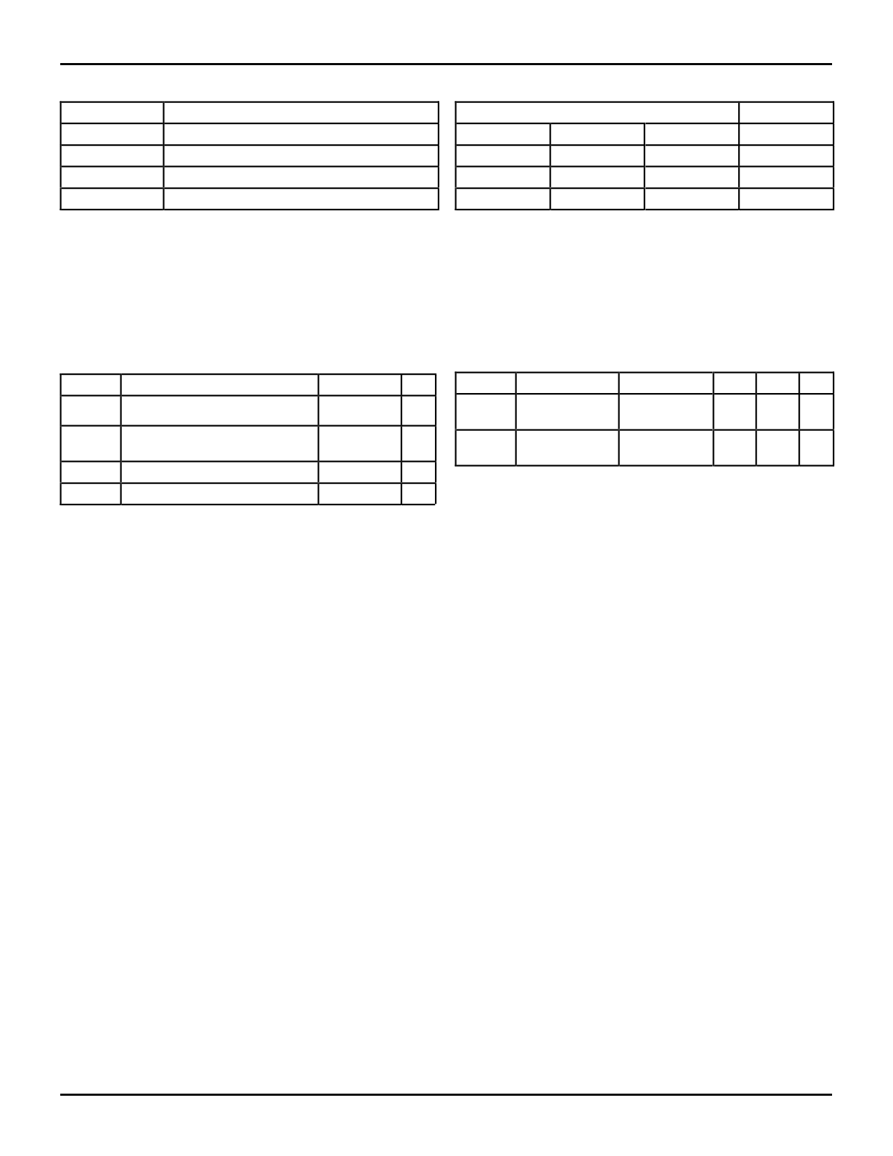
PIN DESCRIPTION
Pin Names
xDx
xLE
xOE
xOx
Data Inputs
Description
Latch Enable Input (Active HIGH)
Output Enable Input (Active LOW)
3-State Outputs
MILITARY AND COMMERCIAL TEMPERATURE RANGES
FUNCTION TABLE(1)
2543 tbl 01
Inputs
xDx
xLE
H
H
L
H
X
X
NOTE:
1. H = HIGH voltage level
L = LOW voltage level
X = Don’t care
Z = High-impedance
xOE
L
L
H
Outputs
xOx
H
L
Z
2543 tbl 02
ABSOLUTE MAXIMUM RATINGS(1)
Symbol
Description
VTERM(2) Terminal Voltage with Respect to
GND
VTERM(3) Terminal Voltage with Respect to
GND
TSTG Storage Temperature
Max.
–0.5 to +7.0
–0.5 to
VCC +0.5
–65 to +150
Unit
V
V
°C
IOUT
DC Output Current
–60 to +120 mA
NOTES:
2543 lnk 03
1. Stresses greater than those listed under ABSOLUTE MAXIMUM RAT-
INGS may cause permanent damage to the device. This is a stress rating
only and functional operation of the device at these or any other conditions
above those indicated in the operational sections of this specification is
not implied. Exposure to absolute maximum rating conditions for
extended periods may affect reliability.
2. All device terminals except FCT162XXXT Output and I/O terminals.
3. Output and I/O terminals for FCT162XXXT.
CAPACITANCE (TA = +25°C, f = 1.0MHz)
Symbol Parameter(1) Conditions Typ. Max. Unit
CIN
Input
VIN = 0V
3.5 6.0 pF
Capacitance
COUT Output
VOUT = 0V 3.5 8.0 pF
Capacitance
NOTE:
2543 lnk 04
1. This parameter is measured at characterization but not tested.
5.7
3
Share Link: 