IDT74FCT2373AT(2009) Ver la hoja de datos (PDF) - Integrated Device Technology
Número de pieza
componentes Descripción
Lista de partido
IDT74FCT2373AT Datasheet PDF : 7 Pages
| |||
IDT74FCT2373AT/CT
FAST CMOS OCTAL TRANSPARENT LATCH
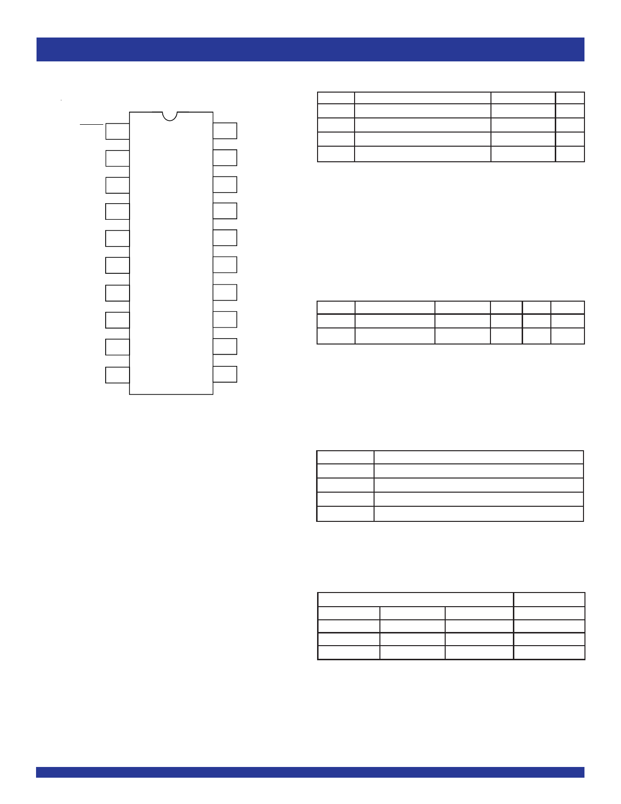
PIN CONFIGURATION
OE
O0
D0
D1
O1
O2
D2
D3
O3
GND
1
20
2
19
3
18
4
17
5
16
6
15
7
14
8
13
9
12
10
11
QSOP
TOP VIEW
VCC
O7
D7
D6
O6
O5
D5
D4
O4
LE
INDUSTRIAL TEMPERATURE RANGE
ABSOLUTE MAXIMUM RATINGS(1)
Symbol
Description
Max
Unit
VTERM(2) Terminal Voltage with Respect to GND
–0.5 to +7
V
VTERM(3) Terminal Voltage with Respect to GND –0.5 to VCC+0.5 V
TSTG Storage Temperature
–65 to +150
°C
IOUT DC Output Current
–60 to +120 mA
NOTES:
1. Stresses greater than those listed under ABSOLUTE MAXIMUM RATINGS may cause
permanent damage to the device. This is a stress rating only and functional operation
of the device at these or any other conditions above those indicated in the operational
sections of this specification is not implied. Exposure to absolute maximum rating
conditions for extended periods may affect reliability. No terminal voltage may exceed
Vcc by +0.5V unless otherwise noted.
2. Inputs and Vcc terminals only.
3. Output and I/O terminals only.
CAPACITANCE (TA = +25°C, F = 1.0MHz)
Symbol
Parameter(1)
Conditions Typ. Max. Unit
CIN
Input Capacitance
VIN = 0V
6
10 pF
COUT
Output Capacitance VOUT = 0V
8
12 pF
NOTE:
1. This parameter is measured at characterization but not tested.
PIN DESCRIPTION
Pin Names
Dx
LE
OE
Ox
Description
Data Inputs
Latch Enable Input (Active HIGH)
Output Enable Input (Active LOW)
3-State Outputs
FUNCTION TABLE(1)
Inputs
Dx
LE
OE
L
H
L
H
H
L
X
X
H
NOTE:
1. H = HIGH Voltage Level
X = Don’t Care
L = LOW Voltage Level
Z = High Impedance
Outputs
Ox
L
H
Z
2
Share Link: 