IN74HCT574A Ver la hoja de datos (PDF) - Integral Corp.
Número de pieza
componentes Descripción
Lista de partido
IN74HCT574A Datasheet PDF : 5 Pages
| |||
IN74HCT574A
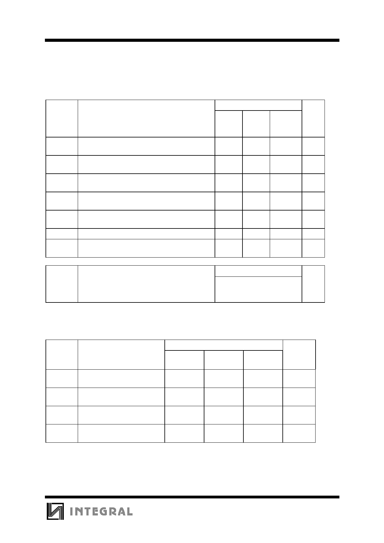
AC ELECTRICAL CHARACTERISTICS(VCC =5.0 V ± 10%, CL=50pF,Input tr=tf=6.0 ns)
Symbol
Parameter
fmax
tPLH, tPHL
tPLZ, tPHZ
tPZH, tPZL
tTLH, tTHL
CIN
COUT
Maximum Clock Frequency (50% Duty Cycle)
(Figures 1 and 4)
Maximum Propagation Delay, Clock to Q
(Figures 1 and 4)
Maximum Propagation Delay, Output Enable to Q
(Figures 2 and 5)
Maximum Propagation Delay, Output Enable to Q
(Figures 2 and 5)
Maximum Output Transition Time, Any Output
(Figures 1 and 4)
Maximum Input Capacitance
Maximum Three-State Output Capacitance
(Output in High-Impedance State)
Guaranteed Limit
25 °C
to
-55°C
≤85°C
≤125°C
30
24
20
30
38
45
28
35
42
28
35
42
12
15
18
10
10
10
15
15
15
Unit
MHz
ns
ns
ns
ns
pF
pF
Power Dissipation Capacitance (Per Flip-Flop)
CPD Used to determine the no-load dynamic power
consumption:
PD=CPDVCC2f+ICCVCC
Typical @25°C,VCC=5.0 V
58
pF
TIMING REQUIREMENTS (VCC =5.0 V ± 10%, CL=50pF,Input tr=tf=6.0 ns)
Guaranteed Limit
Symbol
Parameter
25 °C to
≤85°C
≤125°C
Unit
-55°C
tSU
Minimum Setup Time, Data to
10
13
15
ns
Clock (Figure 3)
th
Minimum Hold Time, Clock
5
5
5
ns
to Data (Figure 3)
tw
Minimum Pulse Width, Clock
15
19
22
ns
(Figure 1)
tr, tf Maximum Input Rise and Fall
500
500
500
ns
Times (Figure 1)
421
Share Link: 