IR2125Z Ver la hoja de datos (PDF) - International Rectifier
Número de pieza
componentes Descripción
Lista de partido
IR2125Z Datasheet PDF : 16 Pages
| |||
IR2125Z
Recommended Operating Conditions
The Input/Output logic timing diagram is shown in Figure 1. For proper operation the device should be
used within the recommended conditions. The VS offset ratings are tested with all supplies biased at
15V differential.
Symbol
Parameter
Min.
Max.
Units
VB
VS
VHO
VCC
VIN
VERR
VCS
High Side Floating Supply Absolute Voltage
High Side Floating Supply Offset Voltage
High Side Floating Output Voltage
Low Side Fixed Supply Voltage
Logic Input Voltage
Error Signal Voltage
Current Sense Signal Voltage
VS + 12
-5
VS + 18
400
VS
VB
12
18
V
VSS
VSS
VS
VCC
VCC
VB
Dynamic Electrical Characteristics
VBIAS (VCC, VBS) = 15V, and CL = 3300 PF and Ta = 25°C unless otherwise specified. The dynamic
electrical characteristics are measured using the test circuit shown in Figure 3 through 6.
Symbol
ton
toff
tr
tf
tcs
tsd
terr
Parameter
Turn-On Propagation Delay
Turn-Off Propagation Delay
Turn-On Rise Time
Turn-Off Fall Time
CS to output shutdown propagation
delay
Shutdown Propagation Delay
CS to ERR pull-up propagation time
Tj = 25°C
Tj =
-55 to 125°C
Min. Typ. Max. Min. Max. Units
150 200 270
150 300 330
ns
43 60 80
26 35 50
0.7 1.2 1.4
1.7 2.2 2.5 µs
9 22 25
Test Conditions
VS = 0V to 400V
CL = 3300pf
VS = 0V TO 400V
Cerr= 270pf
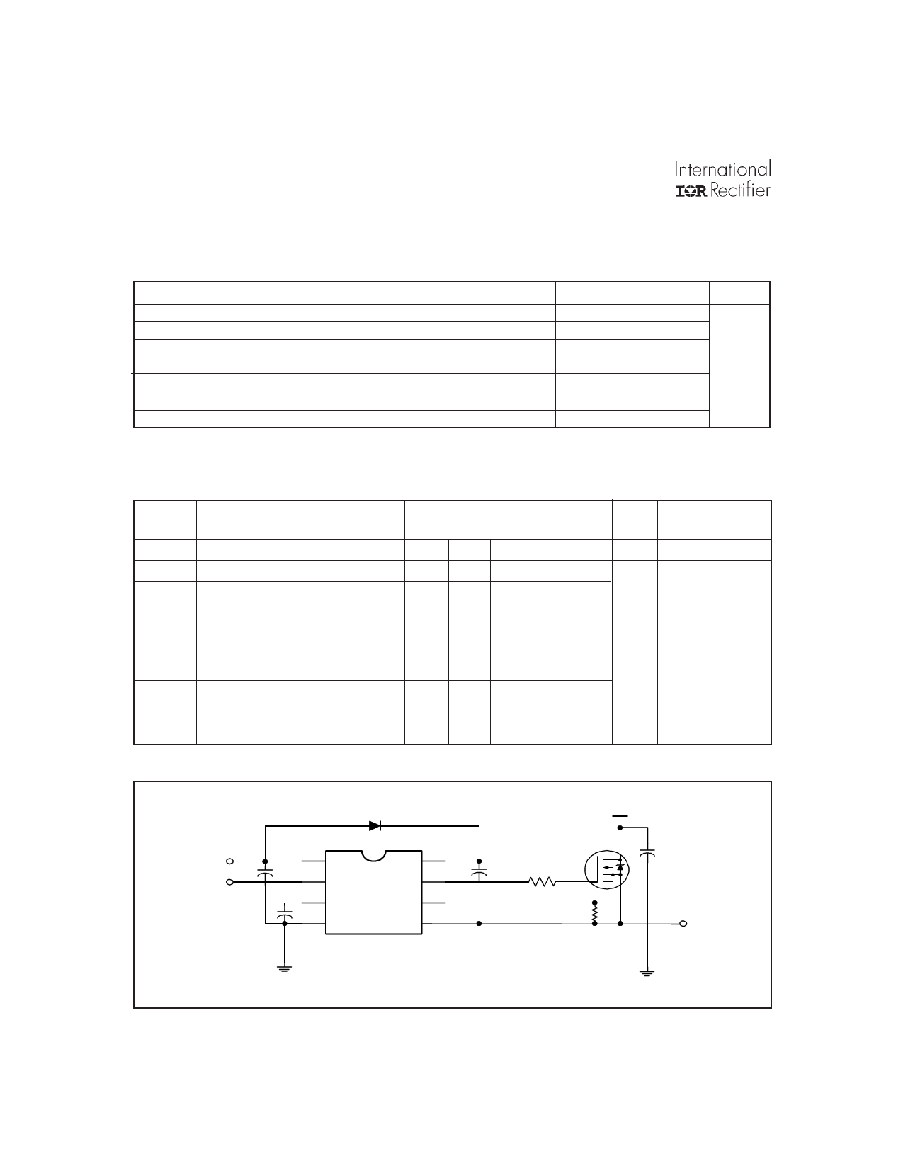
Typical Connection
up to 400V
V CC
V CC
VB
IN
IN
OUT
ERR
CS
COM
VS
TO
LOAD
2
www.irf.com
Share Link: 