IR2136 Ver la hoja de datos (PDF) - International Rectifier
Número de pieza
componentes Descripción
Lista de partido
IR2136 Datasheet PDF : 36 Pages
| |||
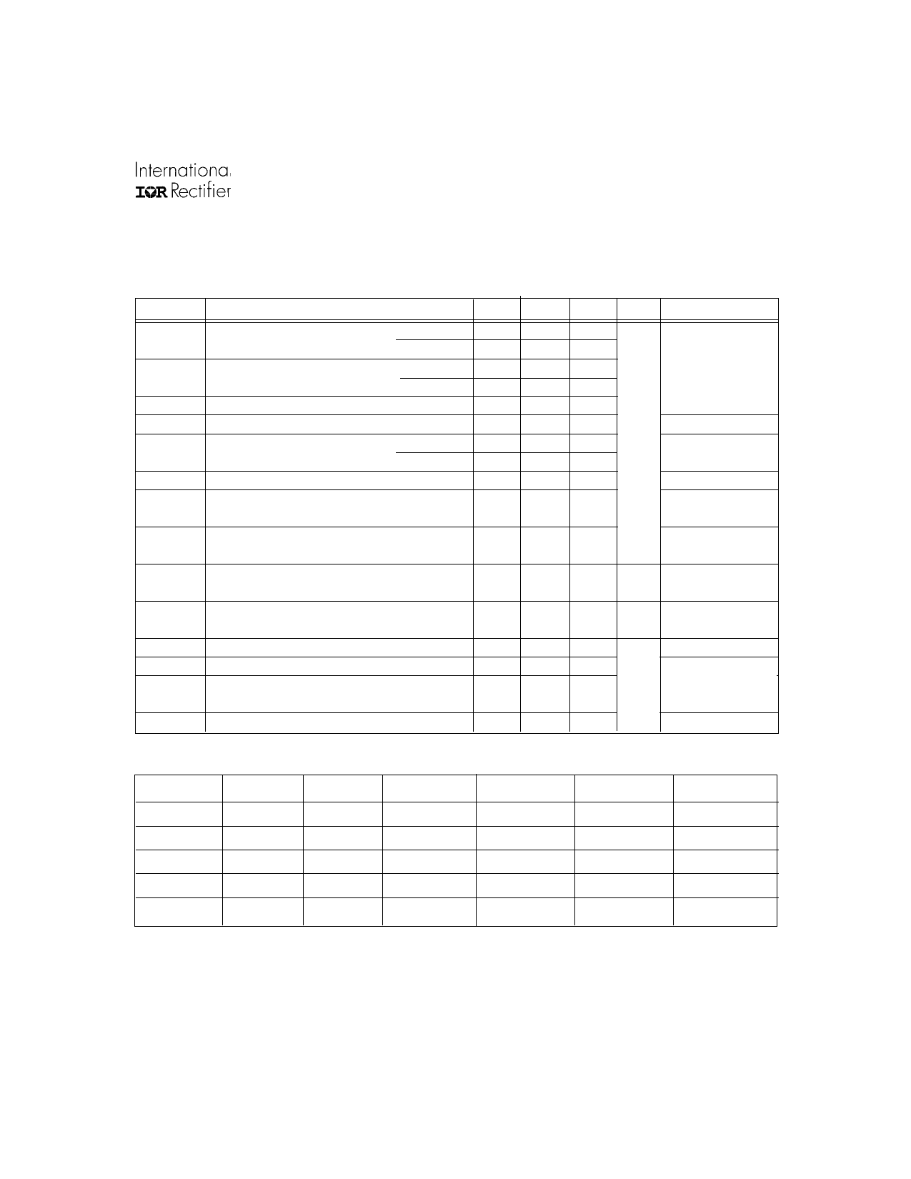
IR2136(2)(3)(5)(6)(7)(8)(J&S) & (PbF)
Dynamic Electrical Characteristics
VCC = VBS = VBIAS = 15V, VS1,2,3 = VSS = COM, TA = 25oC and CL = 1000 pF unless otherwise specified.
Symbol
Definition
Min. Typ. Max. Units Test Conditions
ton
Turn-on propagation delay IR2136(2)(3)(5)(8) 300 425 550
IR21366(7) —
250
—
toff
Turn-off propagation delay IR2136(2)(3)(5)(8) 250 400 550
IR21366(7) —
180
—
VIN = 0 & 5V
tr
Turn-on rise time
—
125
190
tf
Turn-off fall time
—
50
75
tEN
ENABLE low to output
IR2136(2)(3)(5)(8)
300 450
600 nS VIN, VEN = 0V or 5V
shutdown propagation delay
IR21366(7) 100 250 400
tITRIP
tbl
ITRIP to output shutdown propagation delay
ITRIP blanking time
tFLT
ITRIP to FAULT propagation delay
tFILIN
Input filter time (HIN, LIN, EN)
(IR2136(2)(3)(5)(8) only)
500 750
100 150
1000
—
400 600 800
100 200
—
VITRIP = 5V
VIN = 0V or 5V
VITRIP = 5V
VIN = 0V or 5V
VITRIP = 5V
VIN = 0 & 5V
tFLTCLR FAULT clear time RCIN: R=2meg, C=1nF
DT
MT
MDT
Deadtime
Matching delay ON and OFF
Matching delay, max (ton,toff) - min (ton,toff),
(ton,toff are applicable to all 3 channels)
1.3 1.65
220 290
—
40
—
25
2
mS
360
75
70 nS
VIN = 0V or 5V
VITRIP = 0V
VIN = 0 & 5V
External dead
time
>400nsec
PM
Output pulse width matching, PWin -PWout (fig.2) —
40
75
NOTE: For high side PWM, HIN pulse width must be ≥ 1µsec
VCC
<UVCC
15V
15V
15V
15V
VBS
X
<UVBS
15V
15V
15V
ITRIP
X
0V
0V
>VITRIP
0V
ENABLE
X
5V
5V
5V
0V
FAULT
0 (note 1)
high imp
high imp
0 (note 2)
high imp
LO1,2,3
0
LIN1,2,3
LIN1,2,3
0
0
HO1,2,3
0
0
HIN1,2,3
0
0
Note: A shoot-through prevention logic prevents LO1,2,3 and HO1,2,3 for each channel from turning on simultaneously.
Note 1: UVCC is not latched, when VCC>UVCC, FAULT returns to high impedance.
Note 2: When ITRIP <VITRIP, FAULT returns to high-impedance after RCIN pin becomes greater than 8V (@ VCC = 15V)
www.irf.com
5
Share Link: 