IR2137 Ver la hoja de datos (PDF) - International Rectifier
Número de pieza
componentes Descripción
Lista de partido
IR2137 Datasheet PDF : 12 Pages
| |||
IR2137/IR2237(J)(Q)
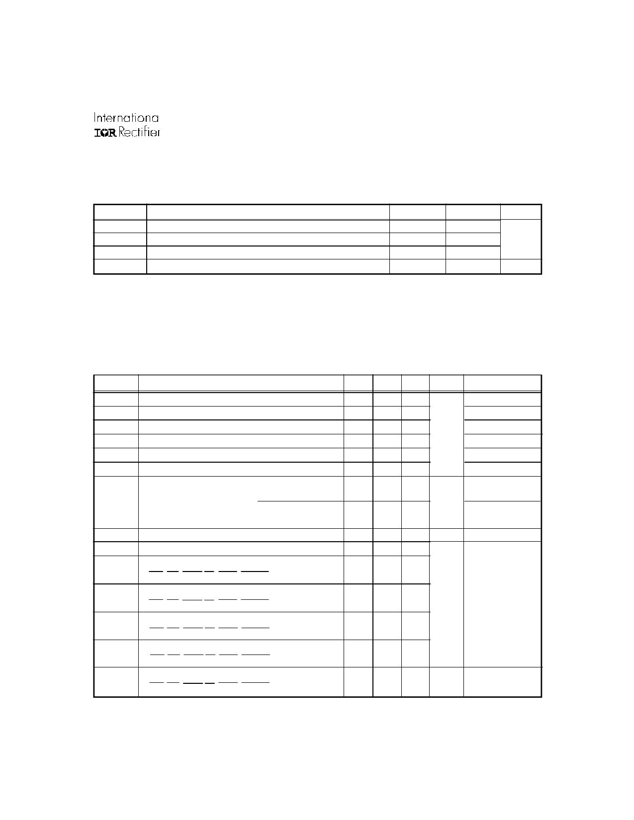
Recommended Operating Conditions
The Input/Output logic timing diagram is shown in figure 1. For proper operation the device should be used within the recom-
mended conditions. All voltage parameters are absolute voltages referenced to COM. The VS offset rating is tested with all
supplies biased at 15V differential.
Symbol
Definition
Min.
Max. Units
VFLT
VLS1,2,3
VDESAT
TA
FAULT output voltage
Low side output return voltage
DESAT pin input voltage
Ambient temperature
VSS
-5.0
VCC
+5.0
V
VS1,2,3
VB1,2,3
-40
125
°C
Note 1: Logic operational for VS of COM -5 to COM +600V/+1200V. Logic state held for VS of COM -5V to -COM VBS.
Note 2: All input pins are internally clamped with a 5.2V zener diode.
Static Electrical Characteristics
VBIAS (VCC, VBS1,2,3) = 15V and TA = 25oC unless otherwise specified. The VIN, V TH and IIN parameters are
referenced to VSS/COM and are applicable to all six channels (HOP/HON1,2,3 and LOP/LON1,2,3). The VO and IO
parameters are referenced to VLS1,2,3 and VS1,2,3 and are applicable to the respective output leads: HO1,2,3 and
LO1,2,3. V DESAT and IDESAT parameters are referenced to VS1,2,3
Symbol
VCCUV+
VCCUV-
VCCUVH
VBSUV+
VBSUV-
VBSUVH
ILK
Definition
VCC supply undervoltage positive going threshold
VCC supply undervoltage negative going threshold
VCC supply undervoltage lockout hysteresis
VBS supply undervoltage positive going threshold
VBS supply undervoltage negative going threshold
VBS supply undervoltage lockout hysteresis
Offset supply leakage current
(IR2137)
(IR2237)
IQBS
IQCC
VIH
VIL
Vt+
Vt-
VT
Quiescent VBS supply current
Quiescent VCC supply current
Logic “0” input voltage (OUT=LO)
(HIN,LIN,ITRIP,SD,BRIN,FLTCLR)
Logic “1” input voltage (OUT=HI)
(HIN,LIN,ITRIP,SD,BRIN,FLTCLR)
Logic input positive going threshold
(HIN,LIN,ITRIP,SD,BRIN,FLTCLR)
Logic input negative going threshold
(HIN,LIN,ITRIP,SD,BRIN,FLTCLR)
Logic input hysteresis
(HIN,LIN,ITRIP,SD,BRIN,FLTCLR)
Min. Typ. Max. Units Test Conditions
10.3 11.4 12.5
9.5 10.4 11.3
—
1.0 —
V
10.3 11.4 12.5
9.5 10.4 11.3
—
1.0 —
—
— 50
VB1,2,3 = VS1,2,3
µA
= 600V
—
— 50
VB1,2,3 = VS1,2,3
= 1200V
— 120 200
—
2
6 mA
3.15 —
—
—
— 0.8
1.6 2.5 3.1
V VCC = 12.5 to 20V
0.9 1.5 2.4
0.7 1.0 —
www.irf.com
3
Share Link: 