IR2010S(2004) Ver la hoja de datos (PDF) - International Rectifier
Número de pieza
componentes Descripción
Lista de partido
IR2010S Datasheet PDF : 16 Pages
| |||
IR2010(S) & (PbF)
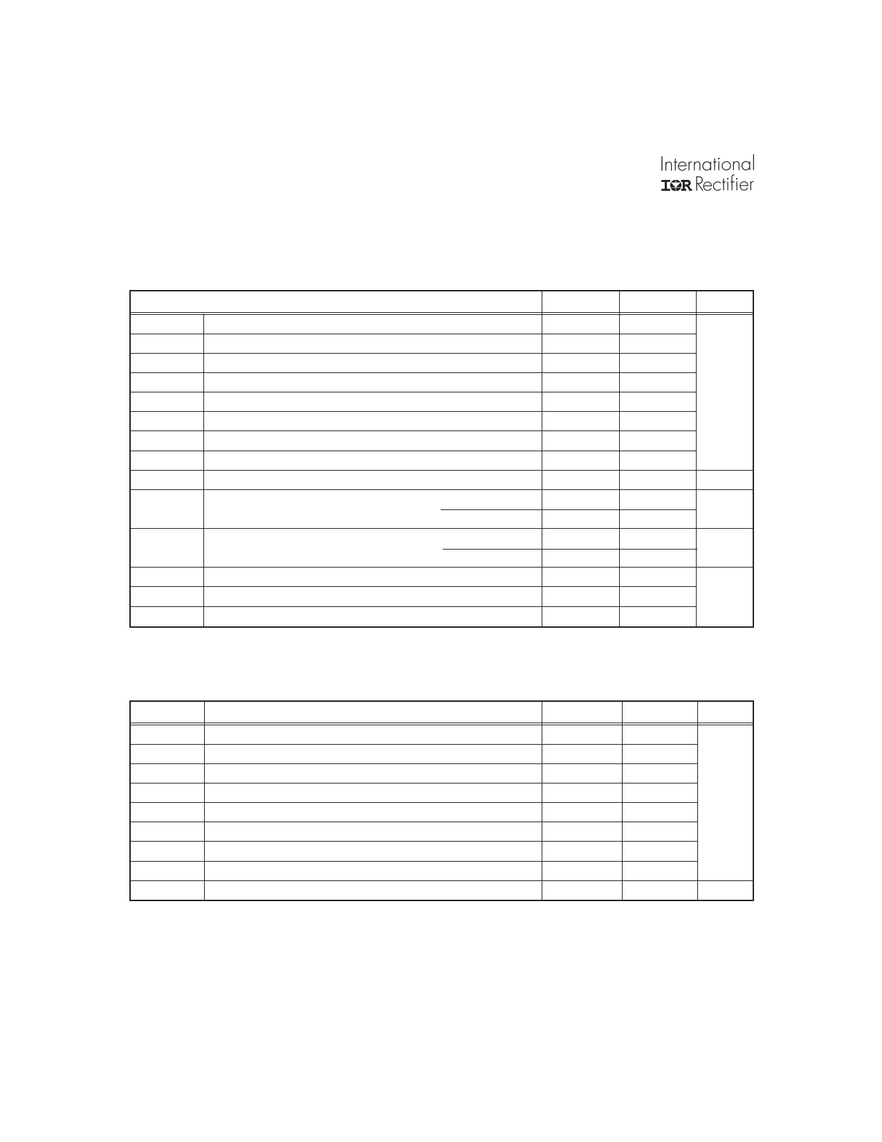
Absolute Maximum Ratings
Absolute maximum ratings indicate sustained limits beyond which damage to the device may occur. All voltage param-
eters are absolute voltages referenced to COM. The thermal resistance and power dissipation ratings are measured
under board mounted and still air conditions.
Symbol
VB
VS
VHO
VCC
VLO
VDD
VSS
VIN
dVs/dt
PD
RTHJA
TJ
TS
TL
Definition
High side floating supply voltage
High side floating supply offset voltage
High side floating output voltage
Low side fixed supply voltage
Low side output voltage
Logic supply voltage
Logic supply offset voltage
Logic input voltage (HIN, LIN & SD)
Allowable offset supply voltage transient (figure 2)
Package power dissipation @ TA ≤ +25°C (14 lead DIP)
(16 lead SOIC)
Thermal resistance, junction to ambient
(14 lead DIP)
(16 lead SOIC)
Junction temperature
Storage temperature
Lead temperature (soldering, 10 seconds)
Min.
-0.3
VB - 25
VS - 0.3
-0.3
-0.3
-0.3
VCC - 25
VSS - 0.3
—
—
—
—
—
—
-55
—
Max.
225
VB + 0.3
VB + 0.3
25
VCC + 0.3
VSS + 25
VCC + 0.3
VDD + 0.3
50
1.6
1.25
75
100
150
150
300
Units
V
V/ns
W
°C/W
°C
Recommended Operating Conditions
The input/output logic timing diagram is shown in figure 1. For proper operation the device should be used within the
recommended conditions. The VS and VSS offset ratings are tested with all supplies biased at 15V differential. Typical
ratings at other bias conditions are shown in figures 24 and 25.
Symbol
Definition
Min.
Max. Units
VB
VS
VHO
VCC
VLO
VDD
VSS
VIN
TA
High side floating supply absolute voltage
High side floating supply offset voltage
High side floating output voltage
Low side fixed supply voltage
Low side output voltage
Logic supply voltage
Logic supply offset voltage
Logic input voltage (HIN, LIN & SD)
Ambient temperature
VS + 10
Note 1
VS + 20
200
VS
VB
10
20
V
0
VCC
VSS + 3
-5 (Note 2)
VSS + 20
5
VSS
VDD
-40
125
°C
Note 1: Logic operational for VS of -4 to +200V. Logic state held for VS of -4V to -VBS.
Note 2: When VDD < 5V, the minimum VSS offset is limited to -VDD.
(Please refer to the Design Tip DT97-3 for more details).
2
www.irf.com
Share Link: 