IR2010(2004) Ver la hoja de datos (PDF) - International Rectifier
Número de pieza
componentes Descripción
Lista de partido
IR2010 Datasheet PDF : 16 Pages
| |||
IR2010(S) & (PbF)
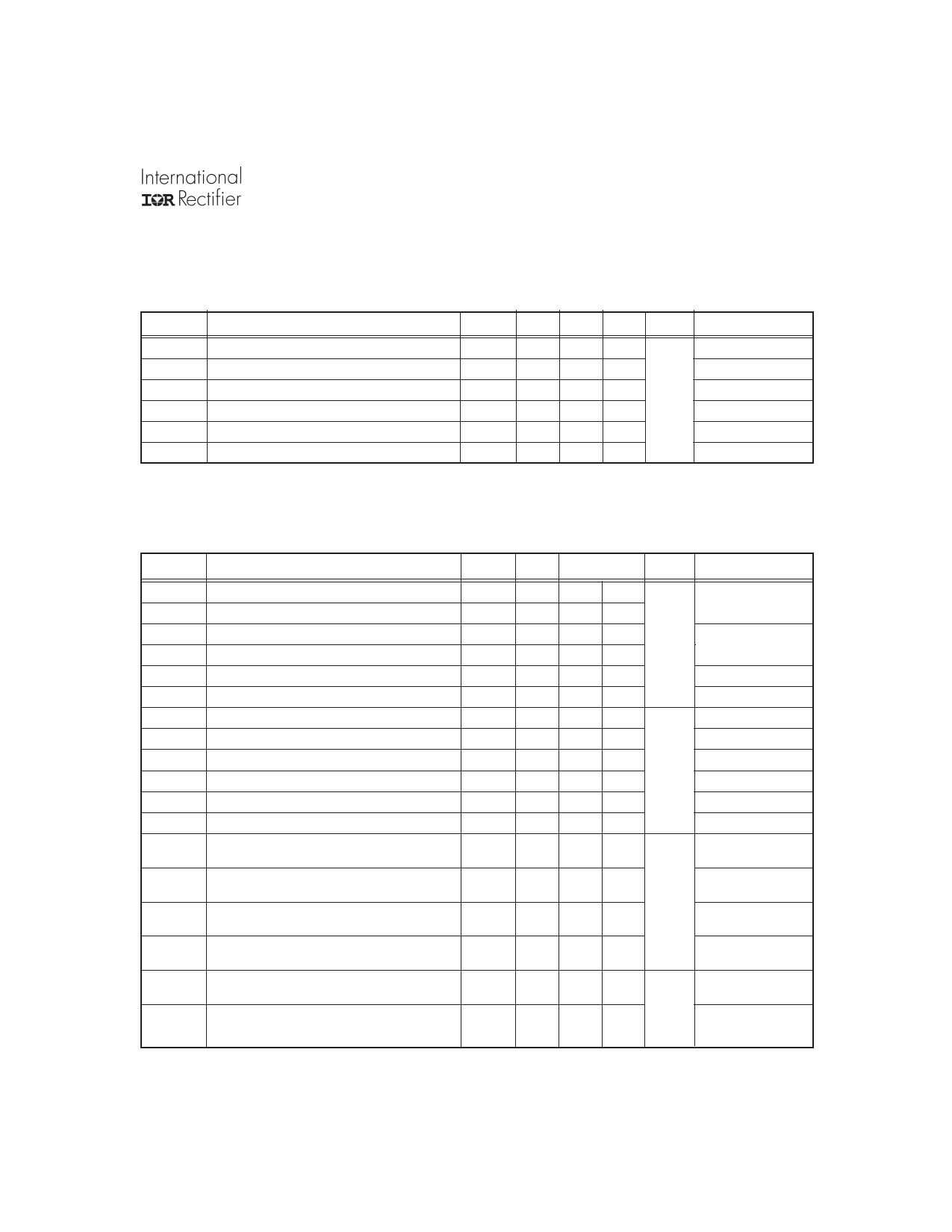
Dynamic Electrical Characteristics
VBIAS (VCC, VBS, VDD) = 15V, CL = 1000 pF, TA = 25°C and VSS = COM unless otherwise specified. The dynamic
electrical characteristics are measured using the test circuit shown in Figure 3.
Symbol
ton
toff
tsd
tr
tf
MT
Definition
Turn-on propagation delay
Turn-off propagation delay
Shutdown propagation delay
Turn-on rise time
Turn-off fall time
Delay matching, HS & LS turn-on/off
Figure Min. Typ. Max. Units Test Conditions
7
50 95 135
8
30 65 105
9
35 70 105
ns
10
—
10 20
VS = 0V
VS = 200V
VS = 200V
11
—
15 25
6
—
— 15
Static Electrical Characteristics
VBIAS (VCC, VBS, VDD) = 15V, TA = 25°C and VSS = COM unless otherwise specified. The VIN, VTH and IIN parameters
are referenced to VSS and are applicable to all three logic input leads: HIN, LIN and SD. The VO and IO parameters are
referenced to COM and are applicable to the respective output leads: HO or LO.
Symbol
VIH
VIL
VIH
VIL
VOH
VOL
ILK
IQBS
IQCC
IQDD
IIN+
IIN-
VBSUV+
VBSUV-
VCCUV+
VCCUV-
IO+
IO-
Definition
Logic “1” input voltage
Logic “0” input voltage
Logic “1” input voltage
Logic “0” input voltage
High level output voltage, VBIAS - VO
Low level output voltage, VO
Offset supply leakage current
Quiescent VBS supply current
Quiescent VCC supply current
Quiescent VDD supply current
Logic “1” input bias current
Logic “0” input bias current
VBS supply undervoltage positive going
threshold
VBS supply undervoltage negative going
threshold
VCC supply undervoltage positive going
threshold
VCC supply undervoltage negative going
threshold
Output high short circuit pulsed current
Output low short circuit pulsed current
Figure Min.
12
9.5
13
—
12
2
13
—
14
—
15
—
16
—
17
—
18
—
19
—
20
—
21
—
22
7.5
Typ. Max. Units Test Conditions
——
— 6.0
VDD = 15V
——
—
1
V
VDD = 3.3V
— 1.0
— 0.1
— 50
70 210
100 230
1
5
µA
20 40
— 1.0
8.6 9.7
IO = 0A
IO = 0A
VB=VS = 200V
VIN = 0V or VDD
VIN = 0V or VDD
VIN = 0V or VDD
VIN = VDD
VIN = 0V
23
7.0 8.2 9.4
V
24
7.5 8.6 9.7
25
7.0 8.2 9.4
26
2.5 3.0 —
VO = 0V, VIN = VDD
PW ≤ 10 µs
27
2.5 3.0 —
A
VO = 15V, VIN = 0V
PW ≤ 10 µs
www.irf.com
3
Share Link: 