IRU1010(2001) Ver la hoja de datos (PDF) - International Rectifier
Número de pieza
componentes Descripción
Lista de partido
IRU1010 Datasheet PDF : 6 Pages
| |||
IRU1010
ABSOLUTE MAXIMUM RATINGS
Input Voltage (Vin) ....................................................
Power Dissipation .....................................................
Storage Temperature Range ......................................
Operating Junction Temperature Range .....................
7V
Internally Limited
-65°C To 150°C
0°C To 150°C
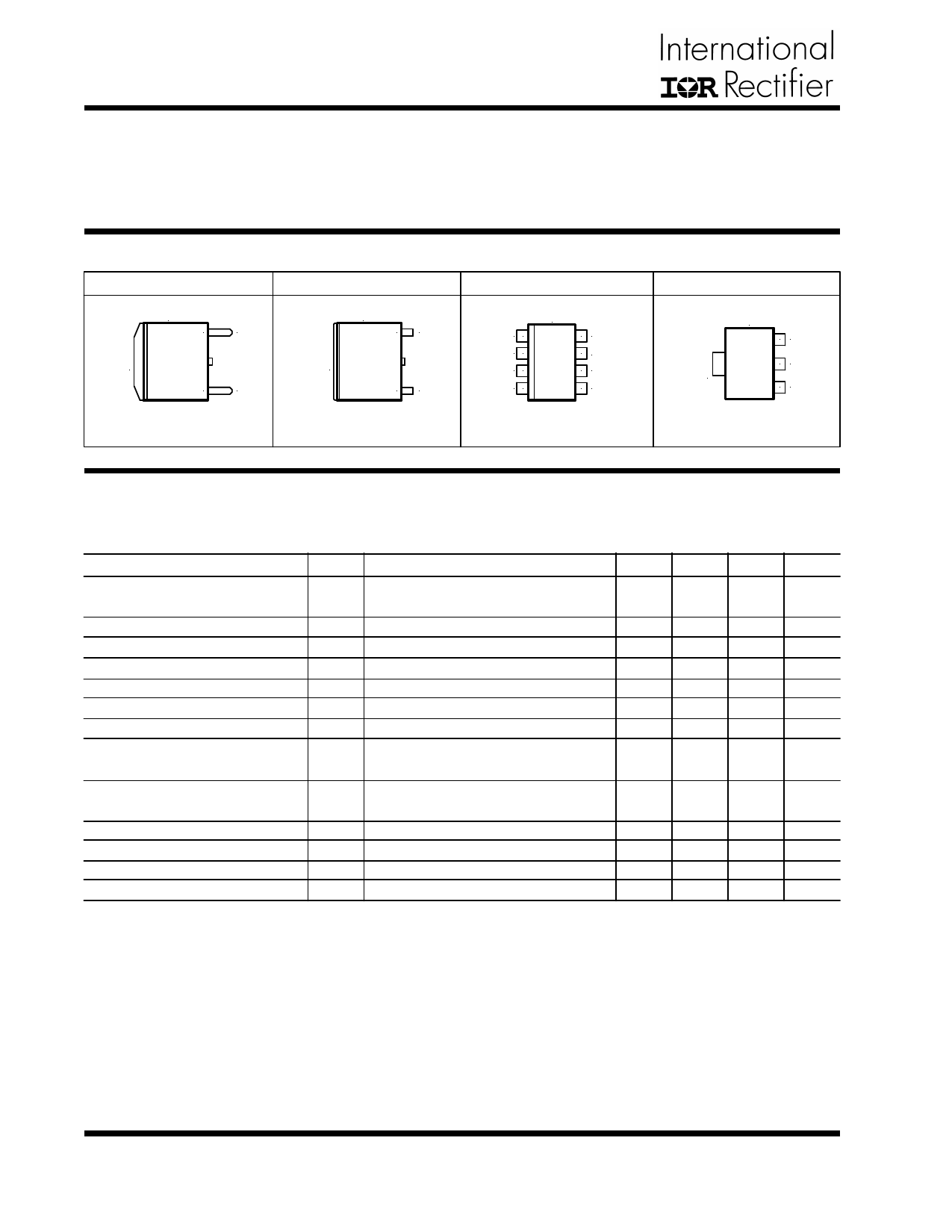
PACKAGE INFORMATION
2-PIN PLASTIC TO-252 (D-Pak) 3-PIN PLASTIC SO-223 (Y)
2-PIN ULTRA THIN-PAK (P)
FRONT VIEW
3
Vin
Tab is
Vout
1
Adj
Tab is
Vout
TOP VIEW
3 Vin
2 Vout
1 Adj
FRONT VIEW
3 Vin
Tab is
Vout
1 Adj
θJA=70!C/W for 0.5" Sq pad
θJA=90!C/W for 0.4" Sq pad
θJA=70!C/W for 0.5" Sq pad
8-PIN PLASTIC SOIC (S)
TOP VIEW
Vin 1
8 Vout
NC 2
7 Vout
NC 3
6 Vout
Adj 4
5 Vout
θJA=55!C/W for 1" Sq pad
ELECTRICAL SPECIFICATIONS
Unless otherwise specified, these specifications apply over Cin=1µF, Cout=10µF, and Tj=0 to 150!C.
Typical values refer to Tj=25!C.
PARAMETER
Reference Voltage
Line Regulation
Load Regulation (Note 1)
Dropout Voltage (Note 2)
Current Limit
Minimum Load Current
(Note 3)
Thermal Regulation
Ripple Rejection
Adjust Pin Current
Adjust Pin Current Change
Temperature Stability
Long Term Stability
RMS Output Noise
SYM
Vref
∆Vo
TEST CONDITION
MIN TYP
Io=10mA, Tj=25!C, (Vin-Vo)=1.5V 1.238 1.250
Io=10mA, (Vin-Vo)=1.5V
1.225 1.250
Io=10mA, 1.3V<(Vin-Vo)<7V
Vin=3.3V, Vadj=0, 10mA<Io<1A
Note 2 , Io=1A
1.1
Vin=3.3V, dVo=100mV
1.1
Vin=3.3V, Vadj=0V
5
MAX
1.262
1.275
0.2
0.4
1.3
10
UNITS
V
%
%
V
A
mA
30ms Pulse, Vin-Vo=3V, Io=1A
f=120Hz, Co=25µF Tantalum,
Io=0.5A, Vin-Vo=3V
Iadj Io=10mA, Vin-Vo=1.5V, Tj=25!C,
Io=10mA, Vin-Vo=1.5V
Io=10mA, Vin-Vo=1.5V, Tj=25!C
Vin=3.3V, Vadj=0V, Io=10mA
Tj=125!C, 1000Hrs
Tj=25!C, 10Hz<f<10KHz
0.01 0.02
60 70
55 120
0.2
5
0.5
0.3
1
0.003
%/W
dB
µA
µA
%
%
%Vo
Note 1: Low duty cycle pulse testing with Kelvin con-
nections is required in order to maintain accurate data.
Note 2: Dropout voltage is defined as the minimum dif-
ferential voltage between Vin and Vout required to main-
tain regulation at Vout. It is measured when the output
voltage drops 1% below its nominal value.
Note 3: Minimum load current is defined as the mini-
mum current required at the output in order for the out-
put voltage to maintain regulation. Typically, the resistor
dividers are selected such that it automatically main-
tains this current.
2
Rev. 1.4
06/29/01
Share Link: 