ISL8204M Ver la hoja de datos (PDF) - Intersil
Número de pieza
componentes Descripción
Lista de partido
ISL8204M Datasheet PDF : 20 Pages
| |||
ISL8204M, ISL8206M
Reference Circuitry For General
Applications
1. Single Power Supply
Figure 15 shows the ISL8204M, ISL8206M
application schematic for input voltage +5V or
+12V. The PVCC pin can connect to the input
supply directly.
CPVCC
RFB RSET-EX
PVCC
COMP/EN
VIN
ISL8204M, ISL8206M
FB
PHASE
ISET
VOUT
PGND
(+5V/+12V)
VIN
CIN
VOUT
COUT
FIGURE 15. TYPICAL APPLICATION SCHEMATIC
2. Separated Power Supply
Figure 16 shows the ISL8204M, ISL8206M
application schematic for wide input voltages from
+1V to +20V. The PVCC supply can source
+5V/+12V or +6.5V to 14.4V.
(+5V/+12V)
or
PVCC
(+6.5V to 14.4V) CPVCC
Note: ISL8204M, ISL8206M has integrated 9.76kΩ
resistance into the module (dividing resistor for top
side). The resistance corresponding to different output
voltages is as shown in Table 2:
TABLE 2. RESISTANCE TO OUTPUT VOLTAGES
VOUT
RFB
0.6V
open
0.8V
28.7kΩ
1.05V
13kΩ
1.2V
9.76kΩ
VOUT
RFB
1.5V
6.49kΩ
1.8V
4.87kΩ
2.5V
3.09kΩ
3.3V
2.16kΩ
VOUT
RFB
5V
1.33kΩ
6V
1.07kΩ
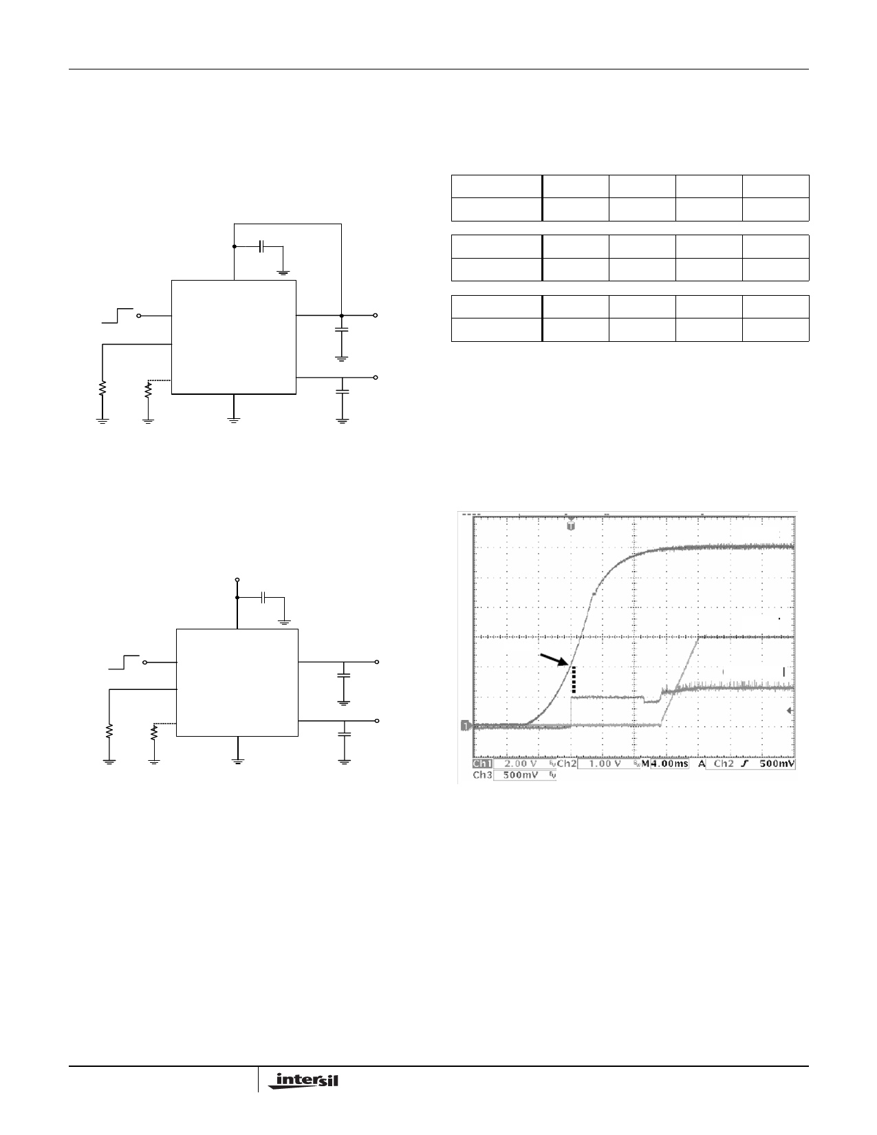
Initialization (POR and OCP Sampling)
Figure 17 shows a start-up waveform of ISL8204M,
ISL8206M. The power-on-reset (POR) function
continually monitors the bias voltage at the PVCC pin.
Once the rising POR threshold has exceeded 4V (VPORR
nominal), the POR function initiates the overcurrent
protection (OCP) sample and hold operation (while
COMP/EN is ~1V). When the sampling is complete, VOUT
begins the soft-start ramp.
PVCC
RFB RSET-EX
PVCC
C O M P /E N
VIN
ISL8204M, ISL8206M
FB
PHASE
ISET
VOUT
PGND
(+1V to +20V)
V IN
C IN
VOUT
COUT
~4V
VOUT
COMP/EN
FIGURE 16. WIDE INPUT VOLTAGE APPLICATION
SCHEMATIC
Applications Information
The typical ISL8204M, ISL8206M application schematic
for input voltage +5V or +12V is shown in Figure 15.
External component selection is primarily determined by
the maximum load current and input/output voltage.
Programming the Output Voltage
The ISL8204M, ISL8206M has an internal 0.6V ±1.5%
reference voltage. Programming the output voltage
requires a dividing resistor (RFB). The output voltage can
be calculated as shown in Equation 1:
VOUT = 0.6 × ⎝⎛1 + -9-R--.--7-F--6-B---k-⎠⎞
(EQ. 1)
FIGURE 17. POR AND SOFT-START OPERATION
If the COMP/EN pin is held low during power-up, the
initialization will be delayed until the COMP/EN is
released and its voltage rises above the VENDIS trip point.
Figure 18 and Figure 19 show a typical power-up
sequence in more detail. The initialization starts at T0,
when either PVCC rises above VPORR, or the COMP/EN pin
is released (after POR). The COMP/EN will be pulled up
by an internal 20µA current source, however, the timing
will not begin until the COMP/EN exceeds the VENDIS trip
point (at T1). The external capacitance of the disabling
device, as well as the compensation capacitors, will
determine how quickly the 20µA current source will
charge the COMP/EN pin. With typical values, it should
10
FN6999.1
February 25, 2010
Share Link: 