AIC1570 Ver la hoja de datos (PDF) - Analog Intergrations
Número de pieza
componentes Descripción
Lista de partido
AIC1570
Analog Intergrations

AIC1570 Datasheet PDF : 18 Pages
| |||
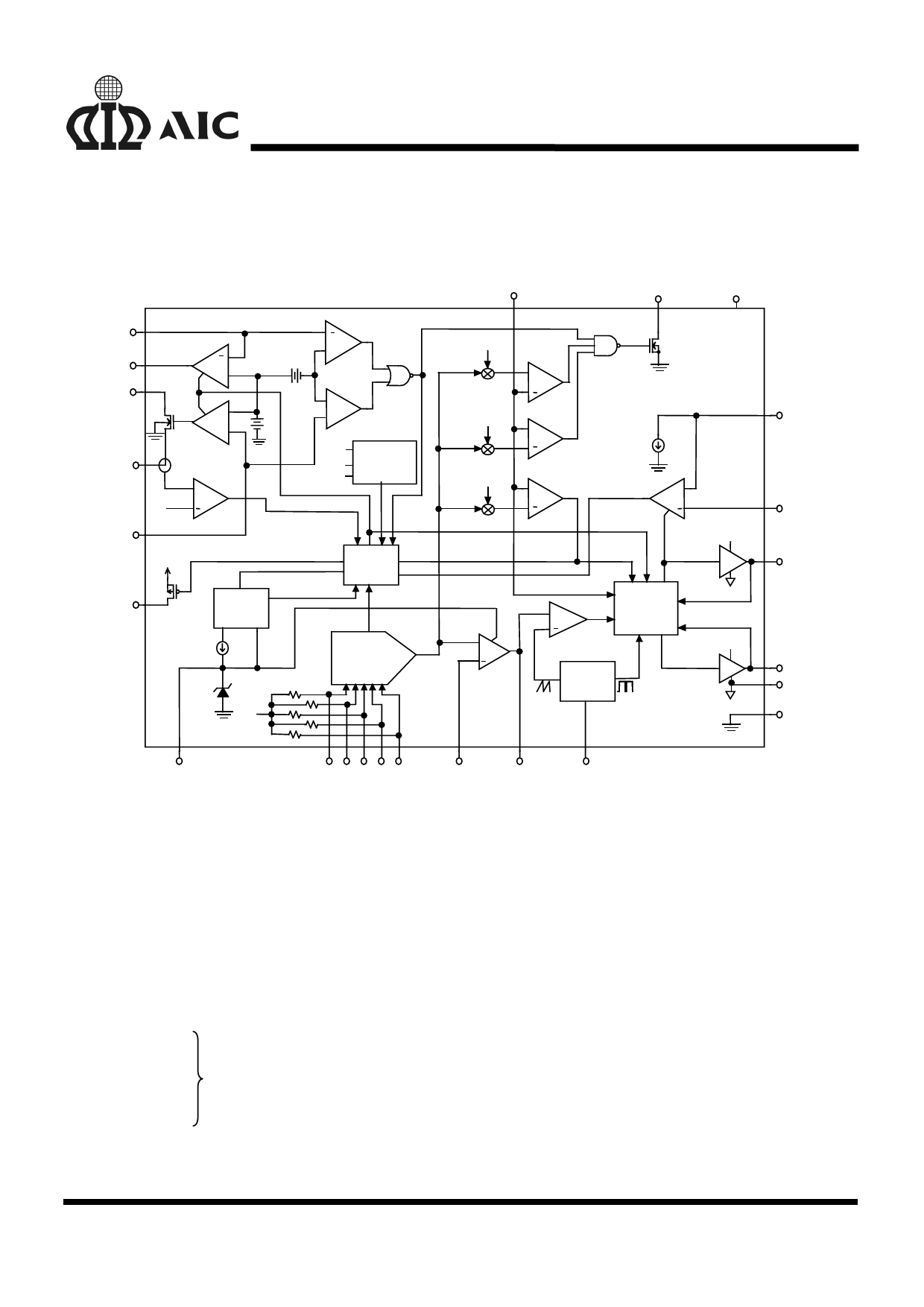
AIC1570
BLOCK DIAGRAM
VSEN
PGOOD
VCC
FB3
GATE3
VIN2
VOUT2
FB2
FAULT
0.5A
+
+
-
+
+
0.3V
+
-
1.26V
VCC
VIN2
OCSET
INHiBIT
OC2
POWER
ON RESET
LUV
VCC
SOFT
START
10µA
4V
5V
FAULT
LOGIC &
LATCH
OFF
70K
70K
70K
70K
70K
5 BIT TTL D/A
CONVERTER
(DAC)
110%
+
90%
+
115%
+
200µA
OC1
+
+
ERROR
AMP
OV
+
GATE CONTROL
PWM COMP
OSCILLATOR
SS
VID0 VID1 VID2 VID3 VID4
FB1
COMP1 RT
VCC
VCC
OCSET
PHASE
UGATE
LGATE
PGND
GND
PIN DESCRIPTIONS
Pin 1: VCC:
Pin 2:
Pin 3:
Pin 4:
Pin 5:
Pin 6:
VID4:
VID3:
VID2:
VID1:
VID0:
The chip power supply pin. It
also provides the gate bias
charge for all the MOSFETs
controlled by the IC.
Recommended supply voltage is
12V.
5bit DAC voltage select pin. TTL
inputs used to set the internal
voltage reference VDAC. When
left open, these pins are
internally pulled up to 5V and
provide logic ones. The level of
VDAC sets the converter output
voltage as well as the PGOOD
and OVP thresholds.
Table 1 specifies the VDAC
voltage for the 32 combinations
of DAC inputs.
Pin 7:
PGOOD: Power good indicator pin.
PGOOD is an open drain output.
This pin is pulled low when the
converter output is ±10% out of
the VDAC reference voltage and
8
Share Link: