K6R1004C1D(2004) Ver la hoja de datos (PDF) - Samsung
Número de pieza
componentes Descripción
Lista de partido
K6R1004C1D Datasheet PDF : 9 Pages
| |||
K6R1004C1D
PRELIMINARY
PRELIMINARY
CMOS SRAM
256K x 4 Bit (with OE) High-Speed CMOS Static RAM
FEATURES
• Fast Access Time 10ns(Max.)
• Power Dissipation
Standby (TTL) : 20mA(Max.)
(CMOS) : 5mA(Max.)
Operating K6R1004C1D-10: 65mA(Max.)
• Single 5.0V±10% Power Supply
• TTL Compatible Inputs and Outputs
• I/O Compatible with 3.3V Device
• Fully Static Operation
- No Clock or Refresh required
• Three State Outputs
• Center Power/Ground Pin Configuration
• Standard Pin Configuration :
K6R1004C1C-J : 32-SOJ-400
K6R1004C1C-K : 32-SOJ-400(Lead-Free)
• Operating in Commercial and Industrial Temperature
range.
GENERAL DESCRIPTION
The K6R1004C1D is a 1,048,576-bit high-speed Static Random
Access Memory organized as 262,144 words by 4 bits. The
K6R1004C1D uses 4 common input and output lines and has
an output enable pin which operates faster than address
access time at read cycle. The device is fabricated using SAM-
SUNG′s advanced CMOS process and designed for high-
speed circuit technology. It is particularly well suited for use in
high-density high-speed system applications. The
K6R1004C1D is packaged in a 400 mil 32-pin plastic SOJ.
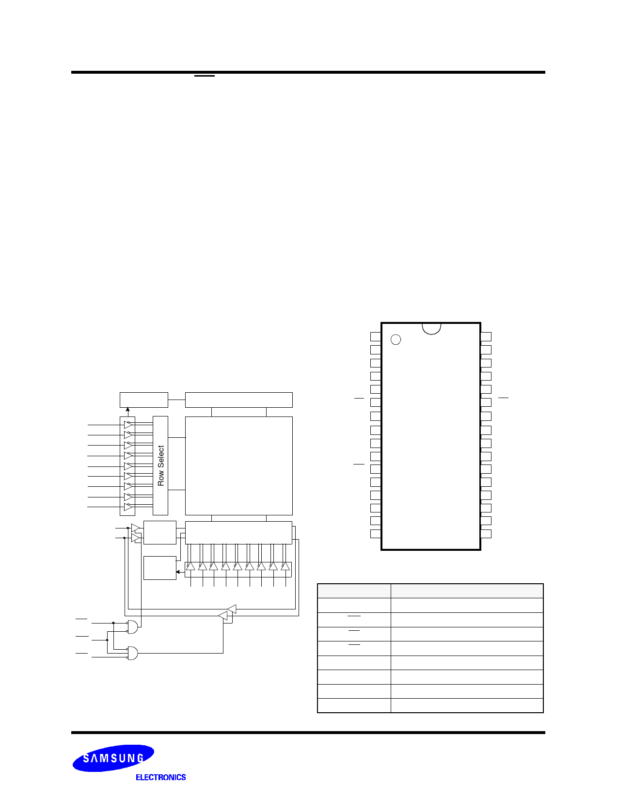
PIN CONFIGURATION(Top View)
FUNCTIONAL BLOCK DIAGRAM
Clk Gen.
A0
A1
A2
A3
A4
A5
A6
A7
A8
I/O1 ~ I/O4
Data
Cont.
Pre-Charge Circuit
Memory Array
512 Rows
512x4 Columns
I/O Circuit &
Column Select
CLK
Gen.
A9 A10 A11 A12 A13 A14 A15 A16 A17
CS
WE
OE
N.C 1
A0 2
A1 3
A2 4
A3 5
CS 6
I/O1 7
Vcc 8
Vss 9
I/O2 10
WE 11
A4 12
A5 13
A6 14
A7 15
N.C 16
SOJ
32 A17
31 A16
30 A15
29 A14
28 A13
27 OE
26 I/O4
25 Vss
24 Vcc
23 I/O3
22 A12
21 A11
20 A10
19 A9
18 A8
17 N.C
PIN FUNCTION
Pin Name
A0 - A17
WE
CS
OE
I/O1 ~ I/O4
VCC
VSS
N.C
Pin Function
Address Inputs
Write Enable
Chip Select
Output Enable
Data Inputs/Outputs
Power(+5.0V)
Ground
No Connection
-3-
Rev. 3.0
July 2004
Share Link: 