L4947PD Ver la hoja de datos (PDF) - STMicroelectronics
Número de pieza
componentes Descripción
Lista de partido
L4947PD Datasheet PDF : 6 Pages
| |||
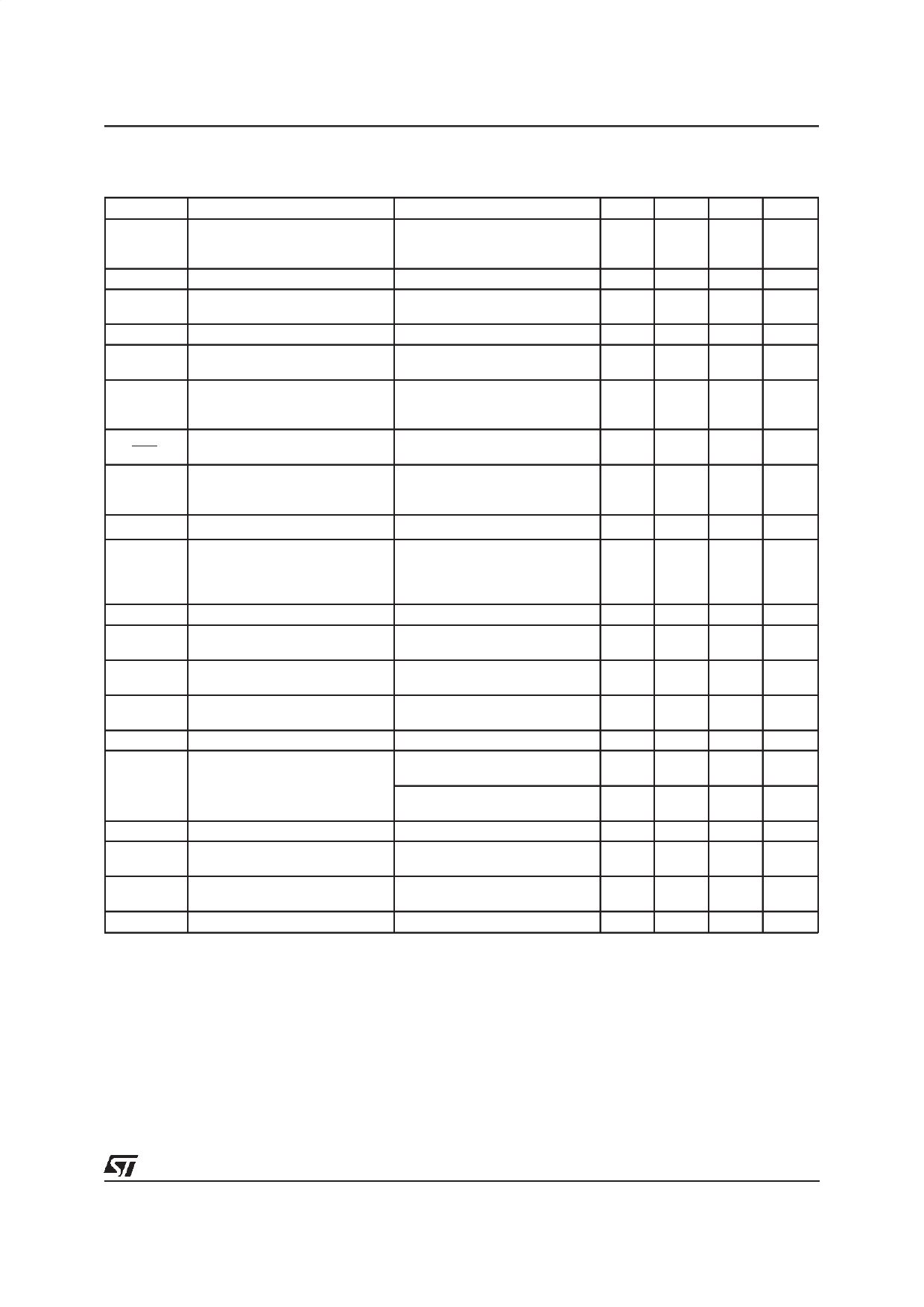
L4947PD
ELECTRICAL CHARACTERISTICS (refer to the test circuit, Vi = 14. 4V, Co = 47µF, ESR < 10Ω,
Rp = 1KΩ, RL = 1KΩ, –40°C ≤ TJ ≤ 125°C, unless otherwise specified)
Symbol
Vo
Vi
∆Vo
∆Vo
Vi –Vo
Iq
∆Vo
T
SVR
Isc
VR
IR
VRT peak
VRT (off)
VRT (on)
VHyst
Vd
VdH
Id
Vdisch
Td
Parameter
Output Voltage
Operating Input Voltage
Line Regulation
Load Regulation
Dropout Voltage
Quiescent Current
Temperature Output Voltage
Drift
Supply Volt. Rej.
Output Short Circuit Current
Test Conditions
Io = 0mA to 500mA
Over Full T Range
TJ = 25°C
Io = 0mA to (*) 500mA
Vi = 6V to 26V ;
Io = 5mA
Io = 5mA to 500mA
Io = 500mA, TJ = 25°C
Over Full T Range
Io = 0mA, TJ = 25°C
Io = 0mA Over Full T
Io = 500mA Over Full T
Io = 350mA ; f = 120Hz
Co = 100µF ;
Vi = 12V ± 5Vpp
Reset Output Saturation Voltage
Reset Output Leakage Current
Power On-Off Reset out Peak
Voltage
Power OFF Vo Threshold
Power ON Vo Threshold
Power ON-Off Hysteresis
Delay Comparator Threshold
Delay Comparator Hysteresis
Delay Capacitor Charging
Current
Delay Capacitor Discharge
Voltage
Power on Reset Delay Time
1.5V < Vo < VRT (off),
IR = 1.6mA
3.0V < Vo < VRT (off),
IR = 8mA
VO in Regulation, VR = 5V
1KΩ Reset Pull-up to Vo
Vo @ Reset Out H to L
Transition
Vo @ Reset Out L to H
Transition
VRT (on) –VRT (off)
Vd @ Reset Out L to H
Transition
Vd @ Reset Out H to L
Transition
Vd = 3V, TJ = 25°C
Vo < VRT (off)
Cd = 100nF, TJ = 25°C
Min. Typ. Max. Unit
4.80 5.00 5.20
V
4.90 5.00 5.10
V
6
26
V
5
50
mV
15
0.40
5
6.5
110
– 0.5
60
mV
0.55
V
0.75
V
10
mA
13
mA
180 mA
mV/°C
50
60
dB
0.50 0.80 1.50
A
0.40
V
0.40
V
50
µA
0.65 1.0
V
4.75 Vo –
0.15
V
VRT (off) Vo –
V
+ 0.05 0.04
0.05
V
3.65 4.00 4.35
V
3.20 3.55 3.90
V
0.45
V
20
/µA
0.55 1.20
V
10
20
30
ms
(*) For a DC voltage 26 < Vi < 37V the device is not operating
FUNCTIONAL DESCRIPTION
The L4947PD is a very low drop 5V/0.5A voltage
regulator provided with a reset function and there-
fore particularly suited to meet the requirements
of supplying the microprocessor systems used in
automotive and industrial applications.
The block diagram shows the basic structure of
the device : the reference, the error amplifier, the
driver, the power PNP, the protection and reset
functions.
The power stage is a Lateral PNP transistor
which allows a very low dropout voltage (typ.
400mV at TJ = 25°C, max. 750mV over the full
temperature range @ IO = 500mA). The typical
curve of the dropout voltage as a function of the
junction temperature is shown in Fig. 1 : that is
the worst case, where IO = 500mA.
The current consumption of the device (quiescent
3/6
Share Link: 