LIS331DLTR(2007) Ver la hoja de datos (PDF) - STMicroelectronics
Número de pieza
componentes Descripción
Lista de partido
LIS331DLTR
(Rev.:2007)
(Rev.:2007)
STMicroelectronics

LIS331DLTR Datasheet PDF : 38 Pages
| |||
Mechanical and electrical specifications
LIS331DL
2.3.2
I2C interface
Subject to general operating conditions for Vdd and top.
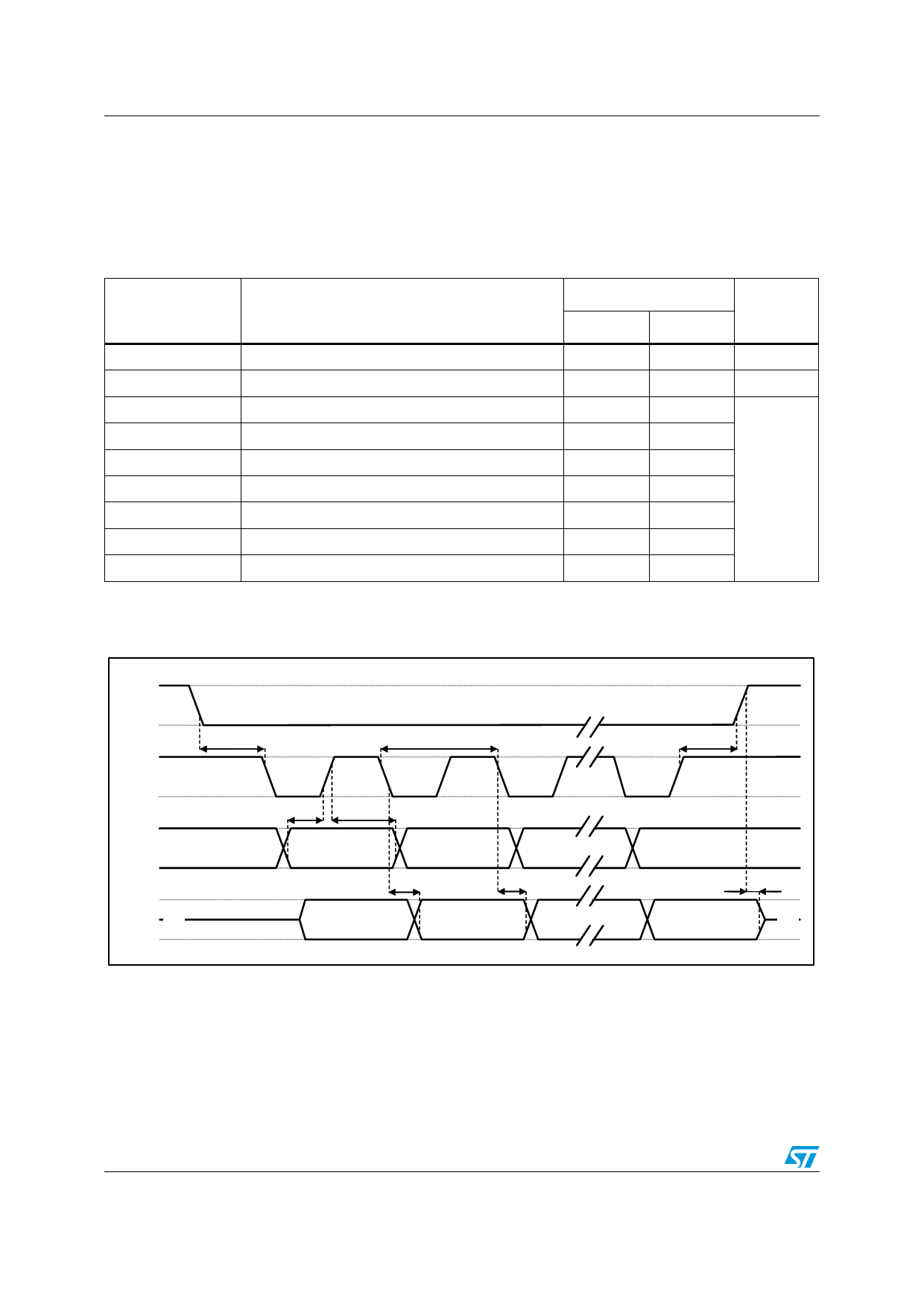
Table 5.
Symbol
I2C Slave timing values
Parameter
I2C standard mode (1)
Min
Max
f(SCL)
SCL clock frequency
0
100
tw(SCLL)
SCL clock low time
4.7
tw(SCLH) SCL clock high time
4.0
tsu(SDA)
th(SDA)
SDA setup time
SDA data hold time
250
0
3.45(2)
tr(SDA) tr(SCL) SDA and SCL rise time
1000
tf(SDA) tf(SCL) SDA and SCL fall time
300
th(ST)
START condition hold time
4
tsu(SR)
Repeated START condition
setup time
4.7
tsu(SP)
STOP condition setup time
4
tw(SP:SR)
Bus free time between STOP
and START condition
4.7
I2C fast mode (1)
Min
Max
0
400
1.3
0.6
100
0
20 + 0.1Cb (3)
20 + 0.1Cb (3)
0.6
0.9(2)
300
300
0.6
0.6
1.3
Unit
KHz
µs
ns
µs
ns
µs
Figure 5. I2C slave timing diagram (4)
START
SDA
REPEATED
START
tsu(SR)
tw(SP:SR)
START
tf(SDA)
SCL
tr(SDA)
tsu(SDA)
th(SDA)
tsu(SP)
STOP
th(ST) tw(SCLL)
tw(SCLH)
tr(SCL)
tf(SCL)
Note: 1 Data based on standard I2C protocol requirement, not tested in production
2 A device must internally provide an hold time of at least 300ns for the SDA signal (referred to
VIHmin of the SCL signal) to bridge the undefined region of the falling edge of SCL
3 Cb = total capacitance of one bus line, in pF
4 Measurement points are done at 0.2·Vdd_IO and 0.8·Vdd_IO, for both port
12/38
Share Link: