3021 Ver la hoja de datos (PDF) - Linear Technology
Número de pieza
componentes Descripción
Lista de partido
3021 Datasheet PDF : 16 Pages
| |||
LT3021/LT3021-1.2/
LT3021-1.5/LT3021-1.8
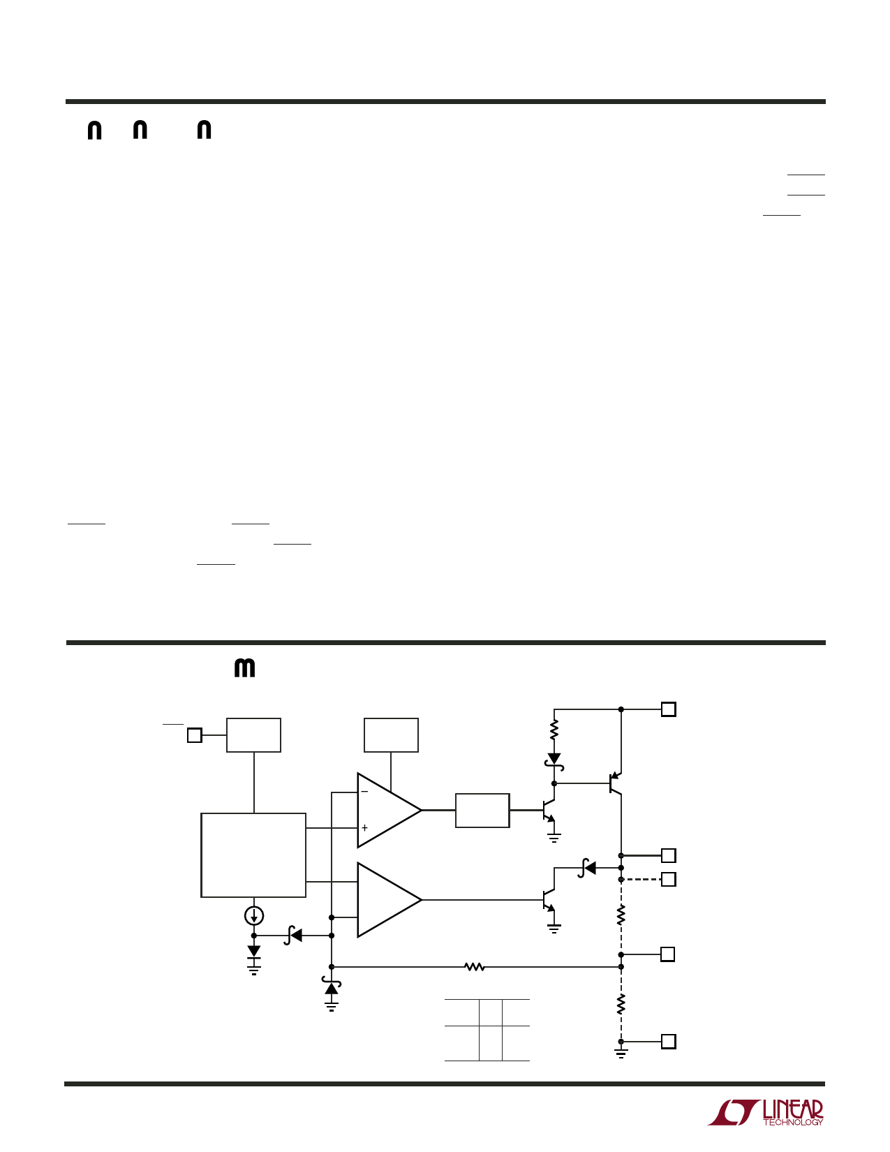
PI FU CTIO S (DH Package/S8 Package)
OUT (Pins 3, 4/Pin 2): These pins supply power to the load.
Use a minimum output capacitor of 3.3µF to prevent oscil-
lations. Applications with large load transients require larger
output capacitors to limit peak voltage transients. See the
Applications Information section for more information on
output capacitance and reverse output characteristics.
SENSE (Pin 7/Pin 3, Fixed Voltage Device Only): This pin
is the sense point for the internal resistor divider. It should
be tied directly to the OUT pins (1, 2) for best results.
ADJ (Pin 7/Pin 3): This pin is the inverting terminal to the
error amplifier. Its typical input bias current of 20nA flows
out of the pin (see curve of ADJ Pin Bias Current vs
Temperature in the Typical Performance Characteristics).
The ADJ pin reference voltage is 200mV (referred to GND).
AGND (Pin 8/Pin 4): Ground.
PGND (Pins 10, 17/Pin 6): Ground.
SHDN (Pin 9/Pin 5): The SHDN pin puts the LT3021 into
a low power state. Pulling the SHDN pin low turns the
output off. Drive the SHDN pin with either logic or an open
collector/drain device with a pull-up resistor. The pull-up
resistor supplies the pull-up current to the open collector/
drain logic, normally several microamperes, and the SHDN
pin current, typically 2.5µA. If unused, connect the SHDN
pin to VIN. The LT3021 does not function if the SHDN pin
is not connected.
IN (Pins 12, 14/Pin 8): These pins supply power to the
device. The LT3021 requires a bypass capacitor at IN if it
is more than six inches away from the main input filter
capacitor. The output impedance of a battery rises with fre-
quency, so include a bypass capacitor in battery-powered
circuits. A bypass capacitor in the range of 3.3µF to 10µF
suffices. The LT3021 withstands reverse voltages on the
IN pin with respect to ground and the OUT pin. In the case
of a reversed input, which occurs if a battery is plugged in
backwards, the LT3021 acts as if a diode is in series with
its input. No reverse current flows into the LT3021 and no
reverse voltage appears at the load. The device protects itself
and the load.
EXPOSED PAD (Pin 17, DH16 Package Only): Ground.
Solder Pin 17 to the PCB ground. Connect directly to Pins
5, 8, 10 for best performance.
NC (Pins 1, 2, 5, 6, 11, 15, 16/Pins 1, 7)
BLOCK DIAGRA (DH Package/S8 Package)
SHDN
(9/5)
SHUTDOWN
BIAS CURRENT
AND
REFERENCE
GENERATOR
200mV
212mV
THERMAL
SHUTDOWN
–
ERROR AMP
+
–
NO-LOAD
RECOVERY
+
CURRENT
GAIN
25k
R3
D1
Q3
Q1
D2
Q2
R2
IN
(12, 14/8)
OUT
(3,4/2)
OUT SENSE
(7/3)
ADJ
(7/3)
8
NOTE:
FOR LT3021 ADJUST PIN (7/3) IS CONNECTED TO
THE ADJUST PIN, R1 AND R2 ARE EXTERNAL.
FOR LT3021-1.X PIN (7/3) IS CONNECTED TO THE
OUTPUT SENSE PIN, R1 AND R2 ARE INTERNAL.
FIXED
VOUT
1.2V
1.5V
1.8V
R1 R2
20k 100k
20k 130k
20k 160k
R1
3021 BD
GND
(8,10,17/4,6)
3021fa
Share Link: 