LT3082 Ver la hoja de datos (PDF) - Linear Technology
Número de pieza
componentes Descripción
Lista de partido
LT3082 Datasheet PDF : 20 Pages
| |||

LT3082
APPLICATIONS INFORMATION
two equal inductors in parallel, but placing them in close
proximity gives the wires mutual inductance adding to
the self-inductance. The second and most effective way
to reduce overall inductance is to place both forward and
return current conductors (the input and GND wires) in
very close proximity. Two 30-AWG wires separated by
only 0.02", used as forward- and return-current conduc-
tors, reduce the overall self-inductance to approximately
one-fifth that of a single isolated wire.
If wiring modifications are not permissible for the applica-
tions, including series resistance between the power supply
and the input of the LT3082 also stabilizes the application.
As little as 0.1Ω to 0.5Ω, often less, is effective in damping
the LC resonance. If the added impedance between the
power supply and the input is unacceptable, adding ESR to
the input capacitor also provides the necessary damping of
the LC resonance. However, the required ESR is generally
higher than the series impedance required.
Paralleling Devices
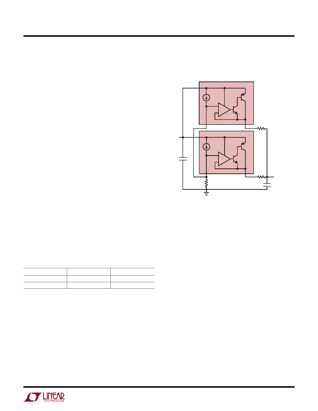
Higher output current is obtained by paralleling multiple
LT3082s together. Tie the individual SET pins together and
tie the individual IN pins together. Connect the outputs in
common using small pieces of PC trace as ballast resistors
to promote equal current sharing. PC trace resistance in
mΩ/inch is shown in Table 2. Ballasting requires only a
tiny area on the PCB.
Table 2. PC Board Trace Resistance
WEIGHT (oz)
10mil WIDTH
1
54.3
2
27.1
Trace resistance is measured in mΩ/in
20mil WIDTH
27.1
13.6
The worst-case room temperature offset, only ±2mV
between the SET pin and the OUT pin, allows the use of
very small ballast resistors.
As shown in Figure 5, each LT3082 has a small 50mΩ
ballast resistor, which at full output current gives better
than 80% equalized sharing of the current. The external
resistance of 50mΩ (25mΩ for the two devices in paral-
lel) adds only about 10mV of output regulation drop at an
output of 0.4A. Even with an output voltage as low as 1V,
this adds only 1% to the regulation. Of course, paralleling
more than two LT3082s yields even higher output current.
Spreading the devices on the PC board also spreads the
heat. Series input resistors can further spread the heat if
the input-to-output difference is high.
IN
LT3082
VIN
4.8V TO
40V
10μA
+
–
SET
IN
LT3082
OUT 50mΩ
10μA
+
1μF
–
SET
165k
OUT 50mΩ
VOUT, 3.3V
0.4A
10μF
3082 F05
Figure 5. Parallel Devices
Quieting the Noise
The LT3082 offers numerous noise performance advan-
tages. Every linear regulator has its sources of noise. In
general, a linear regulator’s critical noise source is the
reference. In addition, consider the error amplifier’s noise
contribution along with the resistor divider’s noise gain.
Many traditional low noise regulators bond out the voltage
reference to an external pin (usually through a large value
resistor) to allow for bypassing and noise reduction. The
LT3082 does not use a traditional voltage reference like
other linear regulators. Instead, it uses a 10μA reference
current. The 10μA current source generates noise current
levels of 2.7pA/√Hz (0.7nARMS over the 10Hz to 100kHz
bandwidth). The equivalent voltage noise equals the RMS
noise current multiplied by the resistor value.
The SET pin resistor generates spot noise equal to √4kTR
(k = Boltzmann’s constant, 1.38 • 10–23J/°K, and T is abso-
lute temperature) which is RMS summed with the voltage
noise If the application requires lower noise performance,
bypass the voltage/current setting resistor with a capacitor
to GND. Note that this noise-reduction capacitor increases
start-up time as a factor of the RC time constant.
3082f
11