LT5537 Ver la hoja de datos (PDF) - Linear Technology
Número de pieza
componentes Descripción
Lista de partido
LT5537 Datasheet PDF : 16 Pages
| |||
LT5537
ELECTRICAL CHARACTERISTICS VCC = 3V, ENBL = 3V, TA = 25°C, unless otherwise specified. (Notes 3, 4)
PARAMETER
Power Supply
Supply Voltage
Supply Current
Shutdown Current
CONDITIONS
(Note 6)
VCC = 3V
ENBL = Low
MIN TYP MAX
2.7
5.25
10
13.5
15
500
UNITS
V
mA
µA
Note 1: Stresses beyond those listed under Absolute Maximum Ratings
may cause permanent damage to the device. Exposure to any Absolute
Maximum Rating condition for extended periods may affect device
reliability and lifetime.
Note 2: Maximum differential AC input voltage between IN+ and IN– is 4V
peak. Equivalent to 22dBm with 50Ω input impedance or 16dBm with
200Ω input impedance (1:4 transformer used).
Note 3: Tests are performed as shown in the configuration of Figure 13.
Note 4: Specifications over the –40°C to 85°C temperature range are
assured by design, characterization and correlation with statistical process
control.
Note 5: Operation at lower frequency is possible as described in the “Low
Frequency Operation” section in Applications Information.
Note 6: The maximum output voltage is limited to approximately VCC –
0.6V. Either the output slope should be reduced or input power level
should be limited in order to avoid saturating the output circuit when VCC <
3V. See discussion in “Dynamic Range” section.
Note 7: Sensitivity is defined as the minimum input power required for the
output voltage to be within 3dB of the ideal log-linear transfer curve.
Sensitivity can be improved by as much as 10dB by using a narrowband
input impedance transformation network. See discussion in “Input
Matching” section.
Note 8: The output slope is adjustable using an external pull-down resistor
(R1). See Applications Information for description of the output circuit.
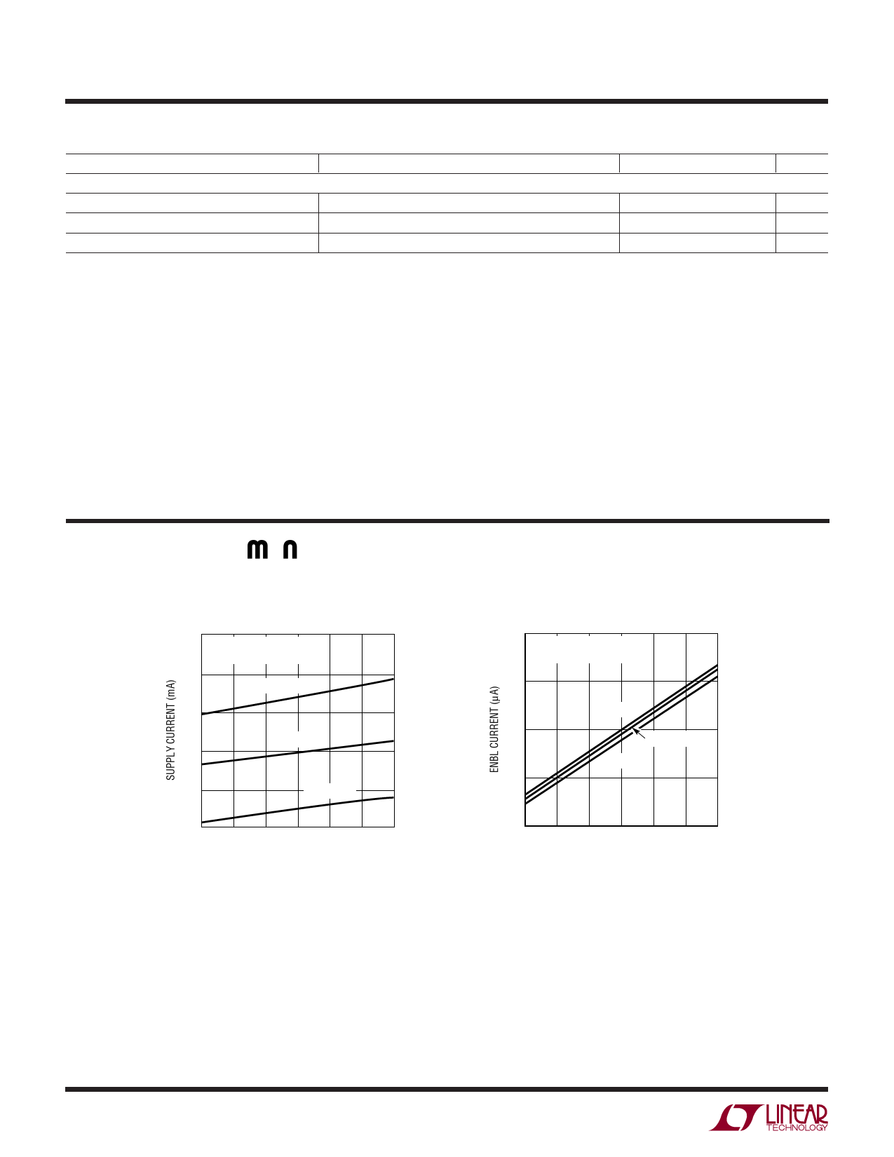
TYPICAL PERFOR A CE CHARACTERISTICS
Supply Current vs Supply Voltage
20
RF INPUT SIGNAL OFF
ENBL = VCC
18
TA = 85°C
16
TA = 25°C
14
12
TA = –40°C
10
2.5
3.0 3.5 4.0 4.5 5.0 5.5
SUPPLY VOLTAGE (V)
5537 G02
ENBL Current vs Supply Voltage
250
RF INPUT SIGNAL OFF
ENBL = VCC
200
TA = 85°C
150
TA = 25°C
TA = –40°C
100
50
2.5
3.0 3.5 4.0 4.5 5.0 5.5
SUPPLY VOLTAGE (V)
5537 G03
5537fa
4
Share Link: 